( ESNUG 582 Item 2 ) ---------------------------------------------- [03/29/18]

Subject: Hogan on Movellus start-up generating custom "digital" analog IP
I predict that meta-simulation will be the center of the looming SPICE
memory simulation battle with the need for high yield and performance
designs.  Its time has come, and it looks like the first SPICE killer
app is Solido High-Sigma Monte Carlo (HSMC).

Game on.

   - Jim Hogan of Vista Ventures LLC
     http://www.deepchip.com/items/0502-08.html
From: [ Jim Hogan of Vista Ventures LLC ]

Hi, John,

It's been nearly 6 years since I gave your readers an update on goings on in
the custom IC/Analog domain.  At the time, I discussed Solido's impact which
continued to evolve as they mastered machine learning and were recently
acquired by Mentor/Siemens.

My interest in analog now is Movellus' industry announcement of analog IP
generators -- initially for PLLs, DLLs and LDOs.


40 YEARS AGO ALL CHIP DESIGN WAS MANUAL/CUSTOM

When I started in the semiconductors industry more than 4 decades years ago,
just as today, designs were fundamentally composed of analog elements and
digital elements.

|

|
|
Analog -- has continuous voltage and continuous current quantities. You design them at the transistor-level with feedback loops. They're very noise sensitive.
|
Digital -- is binary. It's an on-off switch of zeros and ones. These are designed typically a gate-level with open loops. They have a high noise tolerance.
|
The big change since then is...
OVER 40 YEARS DIGITAL CHIP DESIGN BECAME AUTOMATED
Logic synthesis came onto the scene in the late 80s, and digital started
becoming automatic in the late 80s. It became possible to "transform"
information processed from voltage and current waveforms to just zeros and
ones. The on/off switches made it simple to construct circuits using
well-defined gates (ANDs, ORs, etc.), then use Boolean algebra to implement
complicated functions such as add/multiply/subtract/compare etc.
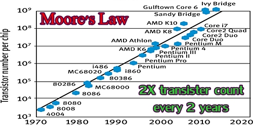
As long as you could speed up the gates by scaling processes, you could
improve the performance of the circuit automatically without much work.
This is essentially what Moore's Law is.  The design stays more-or-less the
same, but the speed of transistors and digital gates increased 2X every 2
years -- and you reaped the benefits with enhanced chip performance.

In digital, you're never optimizing a single transistor or a cell.  The
construction of standard cells allows you to abstract at a higher level
than individual transistors performance.  As a result, digital chip design
has scaled to the point where you can effectively implement millions of
transistors in a few hours or days.


YET IT'S 40 YEARS LATER AND ANALOG DESIGN IS STILL DONE BY HAND?

In contrast to digital design, building even one analog circuit with even
a handful of transistors can take weeks.

Analog's precision requirement has always been tough.  It's heavily
dependent on the impedance of transistors and what kind of current versus
voltage characteristics they have.  You had to optimize the heck out of
every individual transistor, which left no room for abstraction to higher
levels of functionality.

You have complicated transistor-level feedback loops to fine tune and
control all quantities in analog.  Additionally, analog requires resistors,
capacitors, and inductors -- which require additional processing steps, and
thus is not easily amenable to automation.  Analog designers are often
optimizing 10's of different variables in parallel -- human intuition and
experience is important here.


MANUAL ANALOG DESIGN IS A BOTTLENECK IN DIGITAL CHIPS

On digital chips that even have a few small analog blocks, the chip design
teams typically must start designing the analog elements 1-2 years before
the digital elements.

Here are some of the reasons why:

    - Analog's manual design not only takes longer, it also introduces
      more errors.

    - Analog is not process portable.  What worked at 28nm will not work
      at 16nm.  Analog must be redone at new each node.

    - The foundry's process-specific analog models are always later to
      be released than their logic device models.

    - Analog IP must be integrated into the rest of the digital design;
      which creates a whole new set of problems.

    - SPICE verification of an analog block can take 20X longer to verify
      than digital RTL with SystemVerilog.

On top of all theses schedule delays, because DFT cannot be inserted into
analog IP -- fault simulation coverage is zero for analog blocks -- which
is introducing more risk.

The analog elements of a chip design can cause up to 50% of the failures.


EARLY ATTEMPTS AT AUTOMATING ANALOG DESIGN

Over the last 20-30 years, multiple companies have tried to automate analog
chip designs.
In the early 1990's when Texas Instruments and Qualcomm mimicked analog chip
functions by making DSP chips that were coupled with A/D and D/A converters.
This led to Sony Walkmans and iPod/MP3 players.
Neolinear NeoCell and Ciranova both tried to automate analog circuit layout,
and both had some utility.  They used string theory, infinitive instances,
and were hard to optimize.  It took a lot of time and compute power to
solve.  Cadence acquired Neolinear in 2005, and Synopsys acquired Ciranova
in 2012.
Barcelona tried to invent analog synthesis. They succeeded at synthesizing
some small analog blocks such as Op Amps and filters, but even that was not
process portable. And their use of a fixed analog circuit topology limited
its broad usage necessary for an analog designer to re-simulate for variant
implementations. Barcelona folded in 2005.
Antrim did top down synthesis of portable mixed-signal IP. Cadence
acquired Antrim's assets in 2002.
ADA worked at optimizing the transistor devices to meet analog performance
specs. Synopsys acquired ADA in 2004.
While mimicking of analog design made millions for TI and Qualcomm -- it can
be said that each EDA software attempt at automating analog design had
limited utility, or did not scale sufficiently for broad adoption.
WHY NOT AUTOMATE ANALOG FOR THE DIGITAL DESIGNERS?
Since the analog parts of digital chips are holding up everything, why not
create a new catagory of EDA that does analog IP for digital designers?
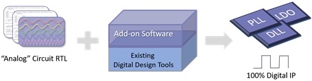
ANNOUNCING THE MOVELLUS ANALOG IP GENERATORS FOR DIGITAL DESIGNERS
The idea is to generate the quality of a handcrafted analog design flow
that's to be used inside your standard digital design flow. It works
by combining proprietary Movellus circuit architectures plus some add-on
Movellus software products to expand your digital synthesis (Design
Compiler and Genus-RTL), static timing analysis (Primetime and Tempus),
and place & route tools (Innovus and ICC/ICC2) to create a 100% digital
implementation of your desired analog functionality.
To use the Movellus Analog IP Generator, in your digital flow you must
process analog "information" the same way you do with digital circuits,
and then abstract out the analog blocks at a much higher level. (That is,
Movellus didn't invent a collection of amplifiers, but instead they created
an entire architectures for the PLLs that don't even require an amplifier.
You just use the Movellus architecture inside your digital flow.)
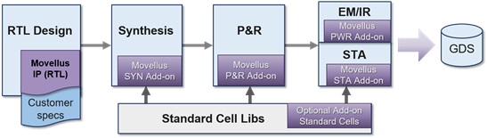
Here's how the Movellus flow works:
Once the Movellus Analog IP Generator software is installed inside your std
cell digital design flow, the digital designers implement the IP the same
way they do with all their other digital IP (e.g. ARM...).
For example, if you were designing a PLL analog IP using Movellus:
1. Like when you get an ARM core, you tweak the general
Movellus PLL RTL code to fit your specific design specs.
2. You optimize the PLL as just another block in your digital
design. For example, if you want to move a PLL to a
different part of the chip, you don't have to worry about
the I/Os -- your digital tools will take care of it.
Further, Movellus' flexible topologies give you multiple
degrees of freedom during logic synthesis.
3. You verify your PLL using your standard Verilog simulators
and/or emulators and/or prototypers.
4. Insert standard DFT/scan for observability and testability.
5. (Optional) - You can further improve performance and power
of your Movellus generated analog IP by adding special
standard cells. (If you do this it adds only two weeks,
vs. several months to handcraft the equivalent analog IP).
Again, remember it's digital tool agnostic. It can support Design Compiler,
Genus-RTL, Primetime, Tempus, Innovus, ICC/ICC2, Calibre, VCS, IES, Questa,
Palladium, Veloce, Zebu, Protium.
THE UNEXPECTED ADVANTAGES OF HAVING "DIGITAL" ANALOG IP
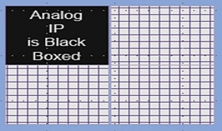
Normally analog IP is a black box in a digital design. This causes a lot of
headaches, including the fact that you can't use your DFT tools on it. The
result is that analog IP can account for 50% of silicon failures.
Because the Movellus-generated analog IP is 100% "digital", you can optimize
it just exactly like the rest of your digital design.  This opens multiple
doors to improving your overall design quality.

    - Analog Power.  System level power consumption can be reduced
      by 5-10%, depending on the design.

      Designers typically take their one main PLL and divide up its
      frequency to generate different frequencies for their many
      different digital IPs which run at different frequencies in their
      chip. (e.g. USB and ARM processor IP).

      By automatically generating previously "analog" PLLs as digital PLLs,
      it dramatically increases the number of available versions of PLLs;
      each with optimized, specific frequencies.  The benefit you don't
      just have a few PLLs -- you can have a tuned PLL for every digital
      block that's optimized for power and performance.

      We've seen this ability to pair digital blocks with their own PLLs
      (thus giving granular power optimization) cut chip-level power
      consumption by 10% to 20%.

    - Analog Jitter.  You can also better optimize your jitter.  Say you
      place your analog PLL in one corner of your SoC and route the high-
      frequencies across the chip, you end up accumulating a lot of jitter
      in the clock tree.  All the noise related to the switching is
      added to the clock.

      If you instead generate digital PLLs, you could put them right next
      to the block that will use the clock, relaxing the jitter budget.

    - Analog Frequency/Performance.  Designers always design their
      digital blocks at a fixed frequency and voltage, because frequency
      comes from the PLL -- and analog is considered black magic.

      Rather than assuming a fixed frequency, and doing timing closure
      with that frequency, if you can implement the PLL in digital, you
      can start co-optimizing all the frequency and margin factors that
      constrain the digital block.  This opens free frequency and margin
      that's leftover -- which enables even more optimization.

    - Analog Area.  The analog functionality implemented using digital
      methods is typically 4-8x smaller because the passives (resistors,
      capacitors, inductors) are eliminated and there is no need for
      carefully crafted precise bias currents and voltages.

    - Analog DFT.  By implementing the "analog" functionality as digital,
      you create degrees of freedom that didn't previously exist -- like
      the ability to insert DFT/scan/ATPG as you would in a digital system
      dramatically reduces your risk of failure.

Right now the Movellus Analog IP Generator has silicon proven PLLs, DLLs,
and LDOs at nodes ranging from 130nm to 14nm FinFET -- and has customers
currently working on 10nm and 7nm silicon.


WHY JIM HOGAN INVESTED IN MOVELLUS

A disruptive new EDA start-up that does true analog fidelity input/output
while still inside a 100% digital implementation flow?  And their idea has
been silicon proven by a customer, Mythic, doing hybrid digital/analog
calculations inside FLASH arrays?
  "The Movellus PLL generator allowed us to focus on designing our SoC
   without worrying about any schedule slips due to late manual analog
   customizations needed to meet our goals.  For example, when we needed
   to push a metal stack change, Movellus was able to provide a correct
   IP in a matter of hours."

       - David Fick, Mythic CTO (press release 01/31/2018)

When I invest, I look at 3 factors: the market (size and growth), technology
(capability and uniqueness), and the team.  The market has been there for a
long time, but not addressable until now.  The promise of the technology has
been verified with customers.  I can see how it will scale to many more
types of analog circuits.  And I've watched Mo Faisal and the Movellus team
aggressively pursue the technology and product.

As a result, I invested in Movellus.

   - Jim Hogan
     Vista Ventures LLC                          Mountain View, CA

        ----    ----    ----    ----    ----    ----   ----

Related Articles

    Jim Hogan on 28 nm yield, SPICE memory battle, meta-simulation
Join
Index
Next->Item
|
|