( ESNUG 540 Item 3 ) -------------------------------------------- [05/16/14]
Subject: Bernard Murphy's 47 quick low voltage RTL design tips (Part I)
> In this ESNUG post I wish to examine how the recent trend of dropping the
> on-chip voltage (VDD) -- to cut power -- ripples throughout every stage
> of chip design. Simply put:
>
> Power == (Voltage^2) / Resistance
>
> That is, as a chip's VDD drops linearly, power use drops geometrically.
>
> What follows are the nuances of how dropping to ultra-low voltages (to
> save on power, and while still maintaining performance over a range of
> temperatures) impacts how our chips are designed.
>
> - Jim Hogan
> Vista Ventures, LLC Los Gatos, CA
From: [ Bernard Murphy of Atrenta ]
Hi, John,
Here's a quick brain dump of all of the clever pre-silicon logic design and
architecture tricks I know that engineers use to cut power. I'm pretty sure
I can't do this topic complete justice, but I'll give it my best shot.
---- ---- ---- ---- ---- ---- ----
LOW VOLTAGE / LOW POWER FROM THE TOP
The bird's-eye view - topics relevant to low power/low voltage design:
- Power estimation (you can't optimize what you can't measure,
here pre-silicon)
- Use of mixed threshold voltage (Vt) libraries
- Clock-gating to reduce dynamic power
- What gating means for clock generation and the clock tree
- Voltage and frequency scaling to reduce dynamic power in
performance-insensitive sections of logic
- Power gating and biasing to reduce leakage power
- Power management support in IPs -- memories, CPUs, GPUs,
and others
- Describing and implementing all of this power intent
- Architecture tricks
- Power state switching in hardware and software
- Near/sub-threshold operation
Below, I have a gross qualitative comparison of these techniques in terms of
effort vs impact. These terms are relative -- "low impact" does NOT mean it
is NOT worth doing -- it just means that it gives less return vs. the other
techniques. "High effort" means that you'll need to put a lot of work in to
get the desired impact.
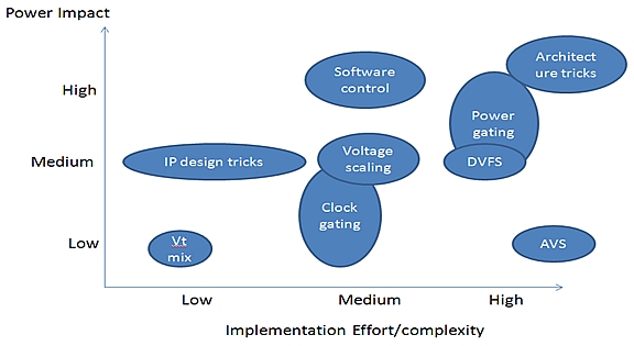 Fig 1: Implementation Effort vs. Complexity
Based on what we see at Atrenta, Vt mix and clock-gating are widely used.
The other techniques are still in early stages of adoption except for very
large consumer-oriented chips such as application processors (TI OMAP,
Qualcomm SnapDragon and others that shall be legally nameless).
---- ---- ---- ---- ---- ---- ----
ESTIMATION
Power estimation is, well, an estimate. The further away you get from
implementation, the less accurate it becomes. Claims are made for Synopsys
PrimeTime-PX (a gate-level estimator and the defacto standard) getting to
within 5% of final silicon power -- though these are often challenged by
complex system behavior and any applications (such as differential power
analysis) which need to understand power as a cycle-level function of time.
In theory, SPICE simulations with layout parasitics would be the best
possible solution, but that's wildly impractical for SoC modeling.
So focus above the gate-level is based on relative guidance -- "is this
implementation better than that?" -- and not so much on absolute accuracy.
That said, you should be able to get RTL-based estimates within 15-20% of
silicon. These tools (our Atrenta SpyGlass Power and Ansys Power Artist
primarily) get highest accuracy using simulation dumps for activity power
estimation. You can also estimate based on "estimated activity" -- but
there you have estimation squared -- which is further reduced in accuracy.
All of these RTL power estimation methods are really for IP and small design
power estimation -- they're limited primarily by tool capacity and how
(un-)representative a simulation can be for modeling a realistic power use.
---- ---- ---- ---- ---- ---- ----
Another method to get to full-chip power estimation is use HW emulation.
1. run emulation,
2. dump all (or most) of the nodes,
3. compute power use based on that dump.
This works, but slows your emulation to a crawl because of the amount of
data it is dumping. Both Mentor Veloce and Cadence Palladium do this.
---- ---- ---- ---- ---- ---- ----
Beyond this, power estimation gets spooky. The most widely used tool for
estimating system power is the Excel spreadsheet. You provide measured power
for existing IPs, RTL or gate-level estimates for new IPs -- and then you
define "use-cases" for the chip which you think are representative of likely
consumer behavior (perhaps you wouldn't be making a phone call at the same
time you are playing Angry Birds, but you might want to browse the web while
you are calling). You then sum power over your active IP's per use-case.
Not exactly high-precision, but close to the state of the art today.
Fig 1: Implementation Effort vs. Complexity
Based on what we see at Atrenta, Vt mix and clock-gating are widely used.
The other techniques are still in early stages of adoption except for very
large consumer-oriented chips such as application processors (TI OMAP,
Qualcomm SnapDragon and others that shall be legally nameless).
---- ---- ---- ---- ---- ---- ----
ESTIMATION
Power estimation is, well, an estimate. The further away you get from
implementation, the less accurate it becomes. Claims are made for Synopsys
PrimeTime-PX (a gate-level estimator and the defacto standard) getting to
within 5% of final silicon power -- though these are often challenged by
complex system behavior and any applications (such as differential power
analysis) which need to understand power as a cycle-level function of time.
In theory, SPICE simulations with layout parasitics would be the best
possible solution, but that's wildly impractical for SoC modeling.
So focus above the gate-level is based on relative guidance -- "is this
implementation better than that?" -- and not so much on absolute accuracy.
That said, you should be able to get RTL-based estimates within 15-20% of
silicon. These tools (our Atrenta SpyGlass Power and Ansys Power Artist
primarily) get highest accuracy using simulation dumps for activity power
estimation. You can also estimate based on "estimated activity" -- but
there you have estimation squared -- which is further reduced in accuracy.
All of these RTL power estimation methods are really for IP and small design
power estimation -- they're limited primarily by tool capacity and how
(un-)representative a simulation can be for modeling a realistic power use.
---- ---- ---- ---- ---- ---- ----
Another method to get to full-chip power estimation is use HW emulation.
1. run emulation,
2. dump all (or most) of the nodes,
3. compute power use based on that dump.
This works, but slows your emulation to a crawl because of the amount of
data it is dumping. Both Mentor Veloce and Cadence Palladium do this.
---- ---- ---- ---- ---- ---- ----
Beyond this, power estimation gets spooky. The most widely used tool for
estimating system power is the Excel spreadsheet. You provide measured power
for existing IPs, RTL or gate-level estimates for new IPs -- and then you
define "use-cases" for the chip which you think are representative of likely
consumer behavior (perhaps you wouldn't be making a phone call at the same
time you are playing Angry Birds, but you might want to browse the web while
you are calling). You then sum power over your active IP's per use-case.
Not exactly high-precision, but close to the state of the art today.
 Also for Excel spreadsheet analysis, it is common to run RTL or gate-level
simulations of your specific design blocks to get more accurate estimates.
---- ---- ---- ---- ---- ---- ----
By the way, if you are using 3rd-party IP, in the eval stage you have to
rely on the IP vendor to give you their "power model". This is a tricky
business. They don't want to give you an overly-pessimistic power model
before you buy, but there is no guarantee their model is representative of
the power usage you later find in your design. Today's fix is you work
very closely with the IP vendor to manage this -- and correct for surprises.
There are tools appearing in the system power space. They all expect you to
provide models for IP -- how you get those models is your problem. The same
applies to your "use-cases". You need to run whatever TLM, virtual model,
or emulation to come up with your realistic use-cases -- or you guess.
Docea is one example, built originally around application processor use-case
modeling, but it is now starting to see some interest in other areas. I see
a challenge for these tools over spreadsheets -- they don't solve the two
biggest problems: IP modeling and use-case development.
---- ---- ---- ---- ---- ---- ----
USING MIXED VT LIBRARIES
This has to be the most widely used and simplest technique, commonly called
MTCMOS, to reduce power. You typically have two cell libraries, one based
on low switching threshold (Vt) cells and the other based on high switching
threshold Vt cells.
Lower Vt cells switch faster, but suffer from higher leakage -- even in an
"off" state. High Vt cells run slower and have lower leakage.
When you synthesize your RTL, you give constraints to guide Design Compiler
or CDNS RTL Compiler to encourage timing-critical logic to be mapped to low
Vt cells and all other remaining logic to be mapped to high Vt cells. This
way you reduce overall leakage power. Your downstream P&R tools will take
care of the power details associated with these choices.
---- ---- ---- ---- ---- ---- ----
CLOCK-GATING
This is the next most widely used technique. The idea is simple -- a high
percentage of logic is inactive at any given time -- but your clock keeps on
triggering each register, even though nothing is changing on most of those
registers. If the clock is disabled on inactive registers, switching power
can be saved. Where and when you can gate a clock depends entirely on
system understanding, so this requires intensive designer input. Both SNPS
Power Compiler and CDNS RTL Compiler provide support for adding clock-gating
during RTL synthesis. You specify which registers should be gated and they
will insert the appropriate clock-gating around those registers.
Atrenta and Calypto (and to some extent Ansys) take this further. If you
know that the clock on a certain register can be gated, then it often
follows that upstream and downstream registers can also be gated, one cycle
earlier or later. It is also sometime possible to "strengthen" clock-
gating -- to keep your specific clock off for longer periods than initially
defined by the engineer -- by looking for stronger implications on the
gating logic. Tools like Synopsys Power Compiler are now clever enough to
automatically optimize clock-gating if given the right constraints.
Also for Excel spreadsheet analysis, it is common to run RTL or gate-level
simulations of your specific design blocks to get more accurate estimates.
---- ---- ---- ---- ---- ---- ----
By the way, if you are using 3rd-party IP, in the eval stage you have to
rely on the IP vendor to give you their "power model". This is a tricky
business. They don't want to give you an overly-pessimistic power model
before you buy, but there is no guarantee their model is representative of
the power usage you later find in your design. Today's fix is you work
very closely with the IP vendor to manage this -- and correct for surprises.
There are tools appearing in the system power space. They all expect you to
provide models for IP -- how you get those models is your problem. The same
applies to your "use-cases". You need to run whatever TLM, virtual model,
or emulation to come up with your realistic use-cases -- or you guess.
Docea is one example, built originally around application processor use-case
modeling, but it is now starting to see some interest in other areas. I see
a challenge for these tools over spreadsheets -- they don't solve the two
biggest problems: IP modeling and use-case development.
---- ---- ---- ---- ---- ---- ----
USING MIXED VT LIBRARIES
This has to be the most widely used and simplest technique, commonly called
MTCMOS, to reduce power. You typically have two cell libraries, one based
on low switching threshold (Vt) cells and the other based on high switching
threshold Vt cells.
Lower Vt cells switch faster, but suffer from higher leakage -- even in an
"off" state. High Vt cells run slower and have lower leakage.
When you synthesize your RTL, you give constraints to guide Design Compiler
or CDNS RTL Compiler to encourage timing-critical logic to be mapped to low
Vt cells and all other remaining logic to be mapped to high Vt cells. This
way you reduce overall leakage power. Your downstream P&R tools will take
care of the power details associated with these choices.
---- ---- ---- ---- ---- ---- ----
CLOCK-GATING
This is the next most widely used technique. The idea is simple -- a high
percentage of logic is inactive at any given time -- but your clock keeps on
triggering each register, even though nothing is changing on most of those
registers. If the clock is disabled on inactive registers, switching power
can be saved. Where and when you can gate a clock depends entirely on
system understanding, so this requires intensive designer input. Both SNPS
Power Compiler and CDNS RTL Compiler provide support for adding clock-gating
during RTL synthesis. You specify which registers should be gated and they
will insert the appropriate clock-gating around those registers.
Atrenta and Calypto (and to some extent Ansys) take this further. If you
know that the clock on a certain register can be gated, then it often
follows that upstream and downstream registers can also be gated, one cycle
earlier or later. It is also sometime possible to "strengthen" clock-
gating -- to keep your specific clock off for longer periods than initially
defined by the engineer -- by looking for stronger implications on the
gating logic. Tools like Synopsys Power Compiler are now clever enough to
automatically optimize clock-gating if given the right constraints.
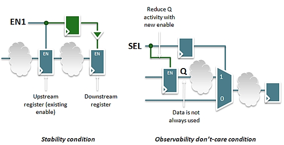 Fig 2: Two ways in which gating can be optimized vs. simple gating.
On the left a downstream register can also be gated (one cycle
later) because the upstream register has been gated. On the
right, a register can be gated under some conditions because
we can prove the register output will not be used under
those conditions.
On most chips, the power used around memory accesses is often a significant
percentage of overall chip power. Power here can be reduced by similar
techniques. For example, there is no need to clock data-in registers to a
RAM if write-enable to the memory is not active.
Fig 2: Two ways in which gating can be optimized vs. simple gating.
On the left a downstream register can also be gated (one cycle
later) because the upstream register has been gated. On the
right, a register can be gated under some conditions because
we can prove the register output will not be used under
those conditions.
On most chips, the power used around memory accesses is often a significant
percentage of overall chip power. Power here can be reduced by similar
techniques. For example, there is no need to clock data-in registers to a
RAM if write-enable to the memory is not active.
 Fig 3: Data input register to a memory can be gated if write-enable
is not active.
Automated techniques like these can save 15% or more power in designs that
have not been carefully tuned by power experts. But they also highlight the
importance of ranking suggested optimizations vs. the estimated power saved,
based on realistic simulations. If a clock needs to turn on and off again
frequently with short periods in the off-state, adding gating logic may
actually increase power.
Fig 3: Data input register to a memory can be gated if write-enable
is not active.
Automated techniques like these can save 15% or more power in designs that
have not been carefully tuned by power experts. But they also highlight the
importance of ranking suggested optimizations vs. the estimated power saved,
based on realistic simulations. If a clock needs to turn on and off again
frequently with short periods in the off-state, adding gating logic may
actually increase power.
 Another thing to watch out for with clock-gating tools -- you better make
sure the changes they make are CDC-safe. There was one notorious example
(I'm not naming names) which probably saved an impressive amount of power
but added lots of new synchronization problems to each design it optimized.
A designer I respect said it "generated evil" because he had to re-run CDC
and undo many of the changes this unnamed tool had made.
---- ---- ---- ---- ---- ---- ----
CLOCK TREE ISSUES
If you're thinking about clock gating, you should also be thinking about
clock generation and your clock tree. The gating I have described so far is
fine-grained or local. You can also consider coarse-grained or more global
gating; for example, gating the main clock input to an IP. The advantage of
coarse-grained clock-gating is you don't just save switching power in the
gates, you also save power in driving the clock sub-tree below that point.
In fact, if you are going to do coarse-grained gating, the higher in the
clock tree you can do that, the more power you will save. Deciding when and
where you can do this takes detailed design understanding and judgment.
If you are thinking about coarse-grained power control, it makes sense to
put clock generation logic and gating in one block near the generating
PLL(s). This might be a little counter-intuitive (you tend to think of
gating the IP clock at the IP), but if you are struggling to cut microAmps,
this can help. And anyway it's good design practice.
---- ---- ---- ---- ---- ---- ----
VOLTAGE & FREQUENCY SCALING
The simplest trick here is to run a part of the logic at a lower voltage if
your chip is not particularly performance critical. Synopsys and ARM derate
some of their memory IP down to 0.9 V for this purpose. Intel and AMD (and
other companies) run non-critical logic in low voltage islands. This is
often called static voltage scaling -- which is in contrast with dynamic
voltage scaling -- more commonly used in dynamic voltage and frequency
scaling (DVFS).
Another thing to watch out for with clock-gating tools -- you better make
sure the changes they make are CDC-safe. There was one notorious example
(I'm not naming names) which probably saved an impressive amount of power
but added lots of new synchronization problems to each design it optimized.
A designer I respect said it "generated evil" because he had to re-run CDC
and undo many of the changes this unnamed tool had made.
---- ---- ---- ---- ---- ---- ----
CLOCK TREE ISSUES
If you're thinking about clock gating, you should also be thinking about
clock generation and your clock tree. The gating I have described so far is
fine-grained or local. You can also consider coarse-grained or more global
gating; for example, gating the main clock input to an IP. The advantage of
coarse-grained clock-gating is you don't just save switching power in the
gates, you also save power in driving the clock sub-tree below that point.
In fact, if you are going to do coarse-grained gating, the higher in the
clock tree you can do that, the more power you will save. Deciding when and
where you can do this takes detailed design understanding and judgment.
If you are thinking about coarse-grained power control, it makes sense to
put clock generation logic and gating in one block near the generating
PLL(s). This might be a little counter-intuitive (you tend to think of
gating the IP clock at the IP), but if you are struggling to cut microAmps,
this can help. And anyway it's good design practice.
---- ---- ---- ---- ---- ---- ----
VOLTAGE & FREQUENCY SCALING
The simplest trick here is to run a part of the logic at a lower voltage if
your chip is not particularly performance critical. Synopsys and ARM derate
some of their memory IP down to 0.9 V for this purpose. Intel and AMD (and
other companies) run non-critical logic in low voltage islands. This is
often called static voltage scaling -- which is in contrast with dynamic
voltage scaling -- more commonly used in dynamic voltage and frequency
scaling (DVFS).
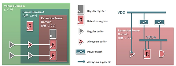 Fig 4: An example of power management configurations
DVFS is a clever technique where you switch both voltage and clock frequency
between a limited set of options, based on performance requirements. In one
mode where you need to run fast, you run at maximum voltage and frequency;
but at higher power. In another "sleepier" mode, you can run slower, at
lower voltage and frequency; so at lower power. Making these choices has
to be a combination of architect/designer know-how and power estimations to
gauge trade-offs.
DVFS has not been widely adopted except in very tightly controlled and
verified IP (ARM uses this method in CPUs) because it creates significant
added complexity in both implementation and verification. You have an IP
that can run at multiple frequencies, so you need synchronization into and
out of that IP. For your design flow, timing closure is more complicated
because you have to consider all corners across each possible frequency.
And in verification, you need to verify not just basic behavior, but also
the behavior at each frequency (perhaps a FIFO works fine at one frequency,
but overflows at another).
A related technique is Adaptive Voltage Scaling (AVS). This is generally
used to adjust for on-chip variation (OCV). Local monitors measure
ring-oscillator frequencies and adjust voltage in a local region to
compensate for process and temperature variation. This can be used to bring
timing back into spec, but also to reduce unnecessary overdrive, hence
power. This is a very advanced technique, typically used only in big
CPU designs since it adds to all of the above problems plus a new wrinkle;
getting design flow timing closure when you don't know how the AVS will
behave in any given case (making corner-case analysis very "interesting").
Fig 4: An example of power management configurations
DVFS is a clever technique where you switch both voltage and clock frequency
between a limited set of options, based on performance requirements. In one
mode where you need to run fast, you run at maximum voltage and frequency;
but at higher power. In another "sleepier" mode, you can run slower, at
lower voltage and frequency; so at lower power. Making these choices has
to be a combination of architect/designer know-how and power estimations to
gauge trade-offs.
DVFS has not been widely adopted except in very tightly controlled and
verified IP (ARM uses this method in CPUs) because it creates significant
added complexity in both implementation and verification. You have an IP
that can run at multiple frequencies, so you need synchronization into and
out of that IP. For your design flow, timing closure is more complicated
because you have to consider all corners across each possible frequency.
And in verification, you need to verify not just basic behavior, but also
the behavior at each frequency (perhaps a FIFO works fine at one frequency,
but overflows at another).
A related technique is Adaptive Voltage Scaling (AVS). This is generally
used to adjust for on-chip variation (OCV). Local monitors measure
ring-oscillator frequencies and adjust voltage in a local region to
compensate for process and temperature variation. This can be used to bring
timing back into spec, but also to reduce unnecessary overdrive, hence
power. This is a very advanced technique, typically used only in big
CPU designs since it adds to all of the above problems plus a new wrinkle;
getting design flow timing closure when you don't know how the AVS will
behave in any given case (making corner-case analysis very "interesting").
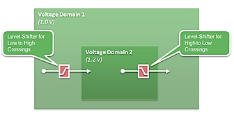 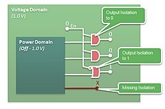 Fig 5: Level shifter and isolation logic needs
When a design has multiple voltage domains or is using DVFS, there will be
signals crossing between different voltage domains -- and that means logic
level shifters are required at least for the low voltage to higher voltage
transitions -- since otherwise a low voltage transition will likely be
insufficient to drive a transition on the high voltage side. (In theory,
you should do the same for high-to-low transitions, in practice we see these
are often being left out, since there usually isn't much of a problem in
overdriving, although there is some power cost).
---- ---- ---- ---- ---- ---- ----
BIASING & POWER GATING
Everything I have described so far, other than Vt mix, is primarily a method
to reduce dynamic power. Leakage power -- the power the device burns even
when it's not doing anything and all the clocks are turned off - is now a
significant component at smaller feature sizes, even more so when a lot of
time is spent in an idle state.
There are fab process ways to alleviate this (FinFET vs FD-SOI) which others
are more qualified to talk about than me. Biasing is another trick. By
changing the bias in the transistor body to something other than power or
ground, you can reduce leakage at the expense of reduced performance. You
can do this statically or dynamically. Also, not my area of expertise so
I'll defer to experts.
Power-gating is one of the most powerful (yeah, I said it) methods to reduce
leakage power. Here you don't just scale voltage -- you turn it off. Doing
this reduces not just dynamic power but also leakage power -- to zero. This
method has been used for many years in major processors, because they have
a lot of functionality that does not need to be on all the time. If you've
ever wondered what "dark silicon" is, this is it -- functions turned off
when not needed. We're now starting to see some interest beyond phone
chips. Wherever you have multiple functions, or a function with multiple
channels -- which do not need to all be on all the time -- you have an
opportunity for power-gating. We also see interest for chips which have
very low (micro-amp) standby power, where the bulk of the functionality is
turned off when not active and only a wakeup function of some kind is
always-on.
There are a couple of wrinkles to using power islands. First, when you
power down a block, you have to isolate it from downstream logic (don't want
floating outputs driving inputs to powered gates). Also, sometimes you
can't quite turn everything off. It might take as much power as you saved
to spin up to a ready state when you re-power the block. In these cases you
insert retention registers (or declare existing registers as retention
registers) which don't turn off when the block turns off. These hold
critical state from which the block can (relatively) quickly recover when
it turns back on.
Second, power and voltage islands create a new design problem not well
covered in power intent descriptions. Both techniques constrain physical
hierarchy, or at least they should. Power rails for a given domain should
ideally be contiguous -- it's wasteful at least in area to have many domains
with identical requirements scattered throughout the floorplan. Each will
require its own power rails and switches. But logic hierarchy is typically
not structured along power boundaries, especially since the power plan may
change quite a bit as the design evolves. In the old days, you would say
"No problem -- we can do all that hierarchy restructuring stuff in the
synthesis or place and route tool". But that was before power intent had
to be described in your RTL to drive P&R implementation downstream. Now you
have a circular dependency. You have to get the hierarchy right, so you can
describe the power intent you want, so you can implement it. If you try to
fix the hierarchy in implementation, your RTL power intent will be wrong --
you'll have level shifter and isolation logic in the wrong places for
example.
Fig 5: Level shifter and isolation logic needs
When a design has multiple voltage domains or is using DVFS, there will be
signals crossing between different voltage domains -- and that means logic
level shifters are required at least for the low voltage to higher voltage
transitions -- since otherwise a low voltage transition will likely be
insufficient to drive a transition on the high voltage side. (In theory,
you should do the same for high-to-low transitions, in practice we see these
are often being left out, since there usually isn't much of a problem in
overdriving, although there is some power cost).
---- ---- ---- ---- ---- ---- ----
BIASING & POWER GATING
Everything I have described so far, other than Vt mix, is primarily a method
to reduce dynamic power. Leakage power -- the power the device burns even
when it's not doing anything and all the clocks are turned off - is now a
significant component at smaller feature sizes, even more so when a lot of
time is spent in an idle state.
There are fab process ways to alleviate this (FinFET vs FD-SOI) which others
are more qualified to talk about than me. Biasing is another trick. By
changing the bias in the transistor body to something other than power or
ground, you can reduce leakage at the expense of reduced performance. You
can do this statically or dynamically. Also, not my area of expertise so
I'll defer to experts.
Power-gating is one of the most powerful (yeah, I said it) methods to reduce
leakage power. Here you don't just scale voltage -- you turn it off. Doing
this reduces not just dynamic power but also leakage power -- to zero. This
method has been used for many years in major processors, because they have
a lot of functionality that does not need to be on all the time. If you've
ever wondered what "dark silicon" is, this is it -- functions turned off
when not needed. We're now starting to see some interest beyond phone
chips. Wherever you have multiple functions, or a function with multiple
channels -- which do not need to all be on all the time -- you have an
opportunity for power-gating. We also see interest for chips which have
very low (micro-amp) standby power, where the bulk of the functionality is
turned off when not active and only a wakeup function of some kind is
always-on.
There are a couple of wrinkles to using power islands. First, when you
power down a block, you have to isolate it from downstream logic (don't want
floating outputs driving inputs to powered gates). Also, sometimes you
can't quite turn everything off. It might take as much power as you saved
to spin up to a ready state when you re-power the block. In these cases you
insert retention registers (or declare existing registers as retention
registers) which don't turn off when the block turns off. These hold
critical state from which the block can (relatively) quickly recover when
it turns back on.
Second, power and voltage islands create a new design problem not well
covered in power intent descriptions. Both techniques constrain physical
hierarchy, or at least they should. Power rails for a given domain should
ideally be contiguous -- it's wasteful at least in area to have many domains
with identical requirements scattered throughout the floorplan. Each will
require its own power rails and switches. But logic hierarchy is typically
not structured along power boundaries, especially since the power plan may
change quite a bit as the design evolves. In the old days, you would say
"No problem -- we can do all that hierarchy restructuring stuff in the
synthesis or place and route tool". But that was before power intent had
to be described in your RTL to drive P&R implementation downstream. Now you
have a circular dependency. You have to get the hierarchy right, so you can
describe the power intent you want, so you can implement it. If you try to
fix the hierarchy in implementation, your RTL power intent will be wrong --
you'll have level shifter and isolation logic in the wrong places for
example.
 Fig 6: Example of grouping two power domains under a new
hierarchy to align with a common power intent for
those domains. Or conversely un-grouping two
domains which may have changed to being in different
power or voltage islands.
There are two ways out of this trap. One is to define the power hierarchy
up-front, before design -- and to forbid any changes beyond that point.
This can work if you can meet your power budget no matter what. But it
isn't practical if you are dealing with large 3rd-party IP (such as the
Imagination Tech GPUs) which must be partitioned for power to meet both a
reasonable budget and reasonable use-cases (you can't just switch the whole
thing on or off). The second approach it to use RTL restructuring. Atrenta
provides a general solution for this. There are other more specialized
solutions from companies such as Magillem.
---- ---- ---- ---- ---- ---- ----
This discussion is continued in part II.
- Bernard Murphy
Atrenta, Inc. San Jose, CA
---- ---- ---- ---- ---- ---- ----
Related Articles
Jim Hogan on how low energy designs will shape everyone's future
Hogan on how ultra low voltage design changes energy and power
Bernard Murphy's 47 quick low voltage RTL design tips (Part I)
Bernard Murphy's 47 quick low voltage RTL design tips (Part II)
Isadore's 28 low voltage timing sign-off & characterization tips
Trent's 12 tips on transistor and full custom low voltage design
Hogan on SNPS, CDNS, Atrenta, CLKDA, Solido as low voltage tools
Fig 6: Example of grouping two power domains under a new
hierarchy to align with a common power intent for
those domains. Or conversely un-grouping two
domains which may have changed to being in different
power or voltage islands.
There are two ways out of this trap. One is to define the power hierarchy
up-front, before design -- and to forbid any changes beyond that point.
This can work if you can meet your power budget no matter what. But it
isn't practical if you are dealing with large 3rd-party IP (such as the
Imagination Tech GPUs) which must be partitioned for power to meet both a
reasonable budget and reasonable use-cases (you can't just switch the whole
thing on or off). The second approach it to use RTL restructuring. Atrenta
provides a general solution for this. There are other more specialized
solutions from companies such as Magillem.
---- ---- ---- ---- ---- ---- ----
This discussion is continued in part II.
- Bernard Murphy
Atrenta, Inc. San Jose, CA
---- ---- ---- ---- ---- ---- ----
Related Articles
Jim Hogan on how low energy designs will shape everyone's future
Hogan on how ultra low voltage design changes energy and power
Bernard Murphy's 47 quick low voltage RTL design tips (Part I)
Bernard Murphy's 47 quick low voltage RTL design tips (Part II)
Isadore's 28 low voltage timing sign-off & characterization tips
Trent's 12 tips on transistor and full custom low voltage design
Hogan on SNPS, CDNS, Atrenta, CLKDA, Solido as low voltage tools
Join
Index
Next->Item
|
|


