( ESNUG 534 Item 3 ) -------------------------------------------- [11/08/13]
Subject: Isadore warns smaller process nodes cause Timing Sign-Off Deadlock
> Each of these groups are caught up in a perpetual tug-of-war against each
> other over margin. During sign-off, they each use margin to pad against
> surprises in timing, clocks, power grids, yield, manufacturing variance,
> and even in the manufacturing delivery time table itself.
>
> At 20 this is no longer realistic. Rule-of-thumb margining is over; there
> is no longer enough margin. Gross percentage adjustments are also over;
> there's no longer enough margin. Gross percentage adjustments for On Chip
> Variation (OCV) from the foundry can run as high as 20%, and when combined
> with padding for clocks, jitter, voltage, and local temps, it's impossible
> to close timing at all corners at your target power and speed.
>
> - Jim Hogan of Vista Ventures
> http://www.deepchip.com/items/0524-04.html
From: [ Isadore Katz of CLKDA ]
Hi John,
Jim Hogan got it right that digital design teams must manage systematic
margining at multiple levels; including sources of variance, derates, and
extensive cell characterization. However, when leading edge SOCs meet
leading edge processes, systematic margining is only part of the challenge
confronting sign-off timing.
This isn't about specific individual features in a Synopsys PrimeTime or
Cadence Tempus -- it's about how you use them. To capture delay and
slack calcs at 28 nm and below, most of the assumptions SoC teams used in
the past are inadequate. Designers must now also consider:
- What are the sign-off corners?
- What's the impact of frontend and backend of line variance?
- What additional electrical effects must now be considered?
Let's look at what's driving the re-examination of today's timing sign-off.
---- ---- ---- ---- ---- ----
MAJOR FACTORS IMPACTING TIMING SIGN-OFF FLOWS
Chip design is a never ending battle to be first to market with the best
functionality, performance, power, price, and volume.
1. The SOC Wars
Problem:
Today it seems like every new chip segment instantaneously becomes
a bar brawl. 8, 9, 10 or more entrants attack a niche; where 1 or
2 players thrive, maybe 3 more players survive.
I've seen this with cellphones, tablets, with Apple, Samsung, Amazon
and Asus as the current surviving big players, and now it's occurring
in the low power servers and networking markets.
The once strong markets leaders like Motorola, Nokia, and Sony have
all seen what a hyper fast moving market and disruptive technology
integration can do to their market share.
 Fig. 1: Global Handset Market Shares
With the SoC design wars, the competitive factors go increasingly
beyond the traditional battle of specs, price and volume delivery.
Consider wireless chips.
- Qualcomm Snapdragon 800 combines: 2.3 Ghz processing,
graphics, DSP for music and audio, modem (with LTE),
USB, Bluetooth, wi-fi, GPS, HD video, 21 megapixel
cameras, and display.
- MediaTek, Nvidia, Broadcom and others are delivering
similar levels of integration.
- Power management and consumption, including the minimum
voltage operating point (0.5 V) impact the competition.
In addition, these same SoC suppliers are fighting for specific
design sockets months in advance of part availability and carrier
contracts: committing to a specification and price comes first,
and then volume delivery must follow.
Impact on design engineers:
Designers are handed nearly impossible tape-out schedules, with
increasing requirements, but unchanged market windows. Most design
teams are already working on the chips that will be in consumers'
hands 12 months from now. For the physical design teams this means
working non-stop for weeks at a time coupled with heroic efforts to
hit timing closure at spec with good yield.
2. Complex Electrical Architectures
Problem:
Demand for ultra-low power, high performance parts along with
integrating different functional and frequency blocks has forced
the combination of multiple voltage, power and clocking domains.
Impact on design engineers:
More engineers are using low-voltage operation, near-threshold
computing, and dynamic voltage scaling to: drive power down,
increase maximum frequency and improve yield. Power management
has led to the adoption of clock gating, turning off blocks, and
other conservation schemes like dark silicon. But it's difficult
to turn off everything -- the turn on and jitter may be more of
a performance hit than any resulting power benefit.
3. Process Node Arms Race
Problem:
Problems 1 and 2 above are creating an "arms race" for SoC houses
and the foundries to put new nodes into volume production as fast
as possible. Each new node from TSMC, Global, Samsung, Intel, IBM
and UMC continues to deliver a material advantage that could not
be achieved architecturally: reduced leakage, better yield-per-wafer,
higher frequency at the same power, and all with greater density.
Moore's Law is slowing down on performance, but it still offers
scaling for power and complexity. There is no choice if you're
in the mobile market but to use leading edge process technology.
Impact on design engineers:
Design teams must now jump on a new node literally as it becomes
available. This means they're betting on foundry maturity curves
in real-time. Libraries and derates may have to be recharacterized
literally a few weeks right before tape-out -- forcing a complete
timing sign-off iteration. Plus the teams are wagering on the node
maturing just in time to hit volume production.
4. Process Variance is now Part of the Flow
Problem:
Small geometries of 28 nm and lower have higher variability both on
Front-End-Of-Line (FEOL) and Back-End-Of-Line (BEOL), causing your
corner-to-corner spread to increase. Pushing a new node into volume
production exposes you to even more of this variability -- which is
understandable given the multi-billion dollar investment of a new
fab and the economic need to fill it quickly.
There is increased process variance both at the device level and on
metal. The following graph illustrates front end of line (FEOL) or
device variance on a basic inverter at 28 nm.
Fig. 1: Global Handset Market Shares
With the SoC design wars, the competitive factors go increasingly
beyond the traditional battle of specs, price and volume delivery.
Consider wireless chips.
- Qualcomm Snapdragon 800 combines: 2.3 Ghz processing,
graphics, DSP for music and audio, modem (with LTE),
USB, Bluetooth, wi-fi, GPS, HD video, 21 megapixel
cameras, and display.
- MediaTek, Nvidia, Broadcom and others are delivering
similar levels of integration.
- Power management and consumption, including the minimum
voltage operating point (0.5 V) impact the competition.
In addition, these same SoC suppliers are fighting for specific
design sockets months in advance of part availability and carrier
contracts: committing to a specification and price comes first,
and then volume delivery must follow.
Impact on design engineers:
Designers are handed nearly impossible tape-out schedules, with
increasing requirements, but unchanged market windows. Most design
teams are already working on the chips that will be in consumers'
hands 12 months from now. For the physical design teams this means
working non-stop for weeks at a time coupled with heroic efforts to
hit timing closure at spec with good yield.
2. Complex Electrical Architectures
Problem:
Demand for ultra-low power, high performance parts along with
integrating different functional and frequency blocks has forced
the combination of multiple voltage, power and clocking domains.
Impact on design engineers:
More engineers are using low-voltage operation, near-threshold
computing, and dynamic voltage scaling to: drive power down,
increase maximum frequency and improve yield. Power management
has led to the adoption of clock gating, turning off blocks, and
other conservation schemes like dark silicon. But it's difficult
to turn off everything -- the turn on and jitter may be more of
a performance hit than any resulting power benefit.
3. Process Node Arms Race
Problem:
Problems 1 and 2 above are creating an "arms race" for SoC houses
and the foundries to put new nodes into volume production as fast
as possible. Each new node from TSMC, Global, Samsung, Intel, IBM
and UMC continues to deliver a material advantage that could not
be achieved architecturally: reduced leakage, better yield-per-wafer,
higher frequency at the same power, and all with greater density.
Moore's Law is slowing down on performance, but it still offers
scaling for power and complexity. There is no choice if you're
in the mobile market but to use leading edge process technology.
Impact on design engineers:
Design teams must now jump on a new node literally as it becomes
available. This means they're betting on foundry maturity curves
in real-time. Libraries and derates may have to be recharacterized
literally a few weeks right before tape-out -- forcing a complete
timing sign-off iteration. Plus the teams are wagering on the node
maturing just in time to hit volume production.
4. Process Variance is now Part of the Flow
Problem:
Small geometries of 28 nm and lower have higher variability both on
Front-End-Of-Line (FEOL) and Back-End-Of-Line (BEOL), causing your
corner-to-corner spread to increase. Pushing a new node into volume
production exposes you to even more of this variability -- which is
understandable given the multi-billion dollar investment of a new
fab and the economic need to fill it quickly.
There is increased process variance both at the device level and on
metal. The following graph illustrates front end of line (FEOL) or
device variance on a basic inverter at 28 nm.
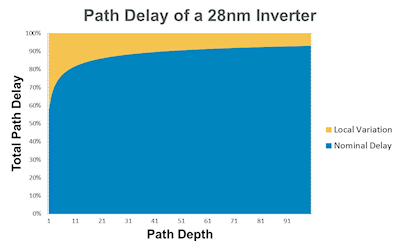 Fig. 2: At lower path depths, variance is >40% of total delay.
More than 40 percent of the delay through the cell can be attributable
to local or on-die variance. This increases the spread between
corners, and requires larger derates (OCV or AOCV). At the smaller
nodes, back end of line (BEOL) double patterning for metallization
has now added even more variability to routing.
Impact on design engineers:
First and foremost, yield! As an example, Apple iPhone 5S demand is
currently limited to the availability of adequate silicon -- their
designers hit timing-closure at spec, but variability is still there.
But variation also has an immediate impact on designers trying to
reach timing closure. The combination of BEOL and FEOL variance,
multi-voltage operating points and traditional temperature points,
results in an explosion in sign-off corners.
There are no longer only 4 corners.
Finding the right corners to run is a major headache. Multiply the
5 standard process corners (SS, SF, FF, FS, TT), by 2 temperature
points, by 4 metal points, and by 4 voltage points. This gives
5*2*4*4 = 160 corners
for sign-off. There are ways to reduce the number of combinations
(for example, only run slow metal at SS for your max frequency), so
no one is running timing at all 160 corners all the time -- but
you're still running a much larger MCMM set than in the past.
The spread between each of the corners is very large due to die-to-die
process variability on metal and device. So even if the number of
corners is reduced, it does not eliminate the designer's problem of
having to satisfy timing in all possible scenarios. These large
on-die variabilities (local variance) result in very large OCV and
AOCV derate factors. This makes it harder to close timing even in
any one corner.
The jury is still out as to the degree of routing metal variability,
but there is no good answer from a sign-off perspective today for
handling BEOL variance, either with corners or statistically.
5. Analog Effects invade Static Timing Analysis for Digital Designs
Problem:
Designers are now beginning to see numerous analog behaviors in
digital circuitry -- low voltage operation, IR variance, clock tree
jitter, Miller capacitance, temperature, stack effects, multiple
input switching and process variance -- that all fall outside of
traditional digital delay and slack analysis.
A few examples of analog factors that impact accuracy which are not
properly captured today in the existing delay modeling like
Synopsys CCS, Cadence ECSM, and non-linear delay models (NLDM).
- Miller capacitances on path receivers
- Constraint variance due to process variation in
registers and latches
- Clock tree jitter due to voltage variation from
multiple frequency domains
- Very long transition times in the active region due
to low voltage operation.
These analog behaviors can impact timing accuracy by 5% or more,
raising serious questions as to what is actually passing or failing.
Impact on design engineers:
The plot below illustrates the impact of process variance on a timing
constraint -- where the timing constraint defines when data and clock
signals must arrive in order for data to be properly captured.
Fig. 2: At lower path depths, variance is >40% of total delay.
More than 40 percent of the delay through the cell can be attributable
to local or on-die variance. This increases the spread between
corners, and requires larger derates (OCV or AOCV). At the smaller
nodes, back end of line (BEOL) double patterning for metallization
has now added even more variability to routing.
Impact on design engineers:
First and foremost, yield! As an example, Apple iPhone 5S demand is
currently limited to the availability of adequate silicon -- their
designers hit timing-closure at spec, but variability is still there.
But variation also has an immediate impact on designers trying to
reach timing closure. The combination of BEOL and FEOL variance,
multi-voltage operating points and traditional temperature points,
results in an explosion in sign-off corners.
There are no longer only 4 corners.
Finding the right corners to run is a major headache. Multiply the
5 standard process corners (SS, SF, FF, FS, TT), by 2 temperature
points, by 4 metal points, and by 4 voltage points. This gives
5*2*4*4 = 160 corners
for sign-off. There are ways to reduce the number of combinations
(for example, only run slow metal at SS for your max frequency), so
no one is running timing at all 160 corners all the time -- but
you're still running a much larger MCMM set than in the past.
The spread between each of the corners is very large due to die-to-die
process variability on metal and device. So even if the number of
corners is reduced, it does not eliminate the designer's problem of
having to satisfy timing in all possible scenarios. These large
on-die variabilities (local variance) result in very large OCV and
AOCV derate factors. This makes it harder to close timing even in
any one corner.
The jury is still out as to the degree of routing metal variability,
but there is no good answer from a sign-off perspective today for
handling BEOL variance, either with corners or statistically.
5. Analog Effects invade Static Timing Analysis for Digital Designs
Problem:
Designers are now beginning to see numerous analog behaviors in
digital circuitry -- low voltage operation, IR variance, clock tree
jitter, Miller capacitance, temperature, stack effects, multiple
input switching and process variance -- that all fall outside of
traditional digital delay and slack analysis.
A few examples of analog factors that impact accuracy which are not
properly captured today in the existing delay modeling like
Synopsys CCS, Cadence ECSM, and non-linear delay models (NLDM).
- Miller capacitances on path receivers
- Constraint variance due to process variation in
registers and latches
- Clock tree jitter due to voltage variation from
multiple frequency domains
- Very long transition times in the active region due
to low voltage operation.
These analog behaviors can impact timing accuracy by 5% or more,
raising serious questions as to what is actually passing or failing.
Impact on design engineers:
The plot below illustrates the impact of process variance on a timing
constraint -- where the timing constraint defines when data and clock
signals must arrive in order for data to be properly captured.
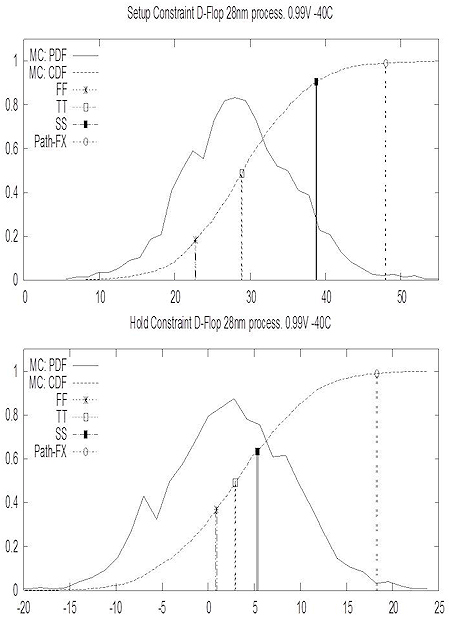 Fig 3. The set-up and hold constraints predicted by TT, SS
and FF, are very optimistic, and the three sigma
constraint (labeled Path FX) is substantially off
to the right.
As the plot shows, the timing constraint predicted by your traditional
corner models is very optimistic. When you account for the process
variance inside of the register, the set-up and hold constraints move
out considerably.
Miller capacitance, also referred to as an active load, describes the
impact of capacitive loading inside of the receiver and effectively
increases the overall capacitive load.
Fig 3. The set-up and hold constraints predicted by TT, SS
and FF, are very optimistic, and the three sigma
constraint (labeled Path FX) is substantially off
to the right.
As the plot shows, the timing constraint predicted by your traditional
corner models is very optimistic. When you account for the process
variance inside of the register, the set-up and hold constraints move
out considerably.
Miller capacitance, also referred to as an active load, describes the
impact of capacitive loading inside of the receiver and effectively
increases the overall capacitive load.
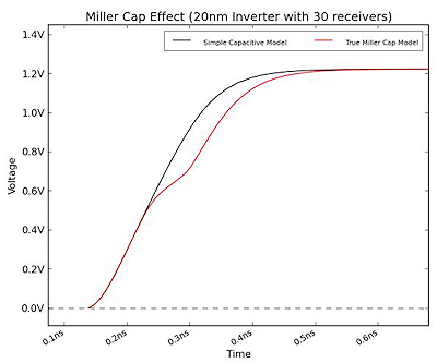
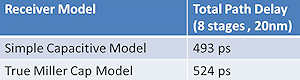 Fig 4. Shows the change in the actual waveform due to Miller
capacitance vs. a simple pin cap. As the delay
comparison shows, the simple pin cap is very optimistic
and can mask timing failures.
Miller capacitance can be the dominant loading effect in some paths at
small geometries, particularly during low voltage operation on paths
with a large number of receivers. However, in CCS the capacitance must
be pre-characterized, and does not properly capture the continuous
impact of dynamic loading.
The chart above illustrates the difference on a path modeled with an
active load to reflect the Miller capacitance and a simple pin cap.
As you can see the simple pin cap is very optimistic and can hide
timing failures.
---- ---- ---- ---- ---- ----
SIGN-OFF DEADLOCK
Problem:
It is becoming almost impossible to close timing in all corners, given the
ambitious (and often conflicting) specs for power and frequency, process
variance, corner spread, large derates -- and the sheer number of PVT
combinations, aka sign-off deadlock. For example, fixing hold violations
in the FF corner creates set-up violations at TT or SS.
Impact on design engineers:
1. They have too many corners to pass. It is very challenging to
get 100+ corners to all pass. Given the spread between the
corners, and very large derates inside of the corners, the gap
between SS, FF, etc. can be impossibly large.
2. Although physical design tools can deliver MCMM optimization,
they can only consider a subset of the corners, which inevitably
means there will be scenarios, and violations that were missed.
3. They must resolve questionable timing accuracy. Because of the
analog effects in the digital logic, the error on the timing can
be +/- 5%. Which means that (a) additional margin has to be
applied to ensure that paths really pass, and (b) teams can
spend a lot of energy arguing over paths that are just passing
or failing timing.
4. SoCs can have millions of timing paths, so the potential that tens
of thousands of paths fail timing in one or more corners is high.
5. There are gaps in sign-off coverage. Between BEOL variance, and
STA accuracy issues (such as low voltage timing), there will be
hidden timing violations that will not be discovered until first
silicon.
The net result is the SoC houses are re-examining their sign-off flows and
assumptions for their newer process nodes. This includes everything from
their selection of sign-off corners, their static timing mode (graph based
or path based), their waiver procedures, their process qualification, their
cell characterization, and their systematic margining.
- Isadore Katz
CLK Design Automation Littleton, MA
Fig 4. Shows the change in the actual waveform due to Miller
capacitance vs. a simple pin cap. As the delay
comparison shows, the simple pin cap is very optimistic
and can mask timing failures.
Miller capacitance can be the dominant loading effect in some paths at
small geometries, particularly during low voltage operation on paths
with a large number of receivers. However, in CCS the capacitance must
be pre-characterized, and does not properly capture the continuous
impact of dynamic loading.
The chart above illustrates the difference on a path modeled with an
active load to reflect the Miller capacitance and a simple pin cap.
As you can see the simple pin cap is very optimistic and can hide
timing failures.
---- ---- ---- ---- ---- ----
SIGN-OFF DEADLOCK
Problem:
It is becoming almost impossible to close timing in all corners, given the
ambitious (and often conflicting) specs for power and frequency, process
variance, corner spread, large derates -- and the sheer number of PVT
combinations, aka sign-off deadlock. For example, fixing hold violations
in the FF corner creates set-up violations at TT or SS.
Impact on design engineers:
1. They have too many corners to pass. It is very challenging to
get 100+ corners to all pass. Given the spread between the
corners, and very large derates inside of the corners, the gap
between SS, FF, etc. can be impossibly large.
2. Although physical design tools can deliver MCMM optimization,
they can only consider a subset of the corners, which inevitably
means there will be scenarios, and violations that were missed.
3. They must resolve questionable timing accuracy. Because of the
analog effects in the digital logic, the error on the timing can
be +/- 5%. Which means that (a) additional margin has to be
applied to ensure that paths really pass, and (b) teams can
spend a lot of energy arguing over paths that are just passing
or failing timing.
4. SoCs can have millions of timing paths, so the potential that tens
of thousands of paths fail timing in one or more corners is high.
5. There are gaps in sign-off coverage. Between BEOL variance, and
STA accuracy issues (such as low voltage timing), there will be
hidden timing violations that will not be discovered until first
silicon.
The net result is the SoC houses are re-examining their sign-off flows and
assumptions for their newer process nodes. This includes everything from
their selection of sign-off corners, their static timing mode (graph based
or path based), their waiver procedures, their process qualification, their
cell characterization, and their systematic margining.
- Isadore Katz
CLK Design Automation Littleton, MA
Join
Index
Next->Item
|
|