( ESNUG 520 Item 1 ) -------------------------------------------- [03/07/13]
From: [ Dean Drako of IC Manage ]
Subject: New data from 372 engineers and managers surveyed on real IP reuse
Hi, John,
IC Manage has has sponsored an annual blind, independent survey for the past
5 years running, with an average of 440 design and verification engineers
participating each year. Approximately 1/2 of the survey respondents are
in engineering management.
NEW IP REUSE DATA
The 2013 survey was completed last month with 372 responses. What follows
is some new data about IP reuse.
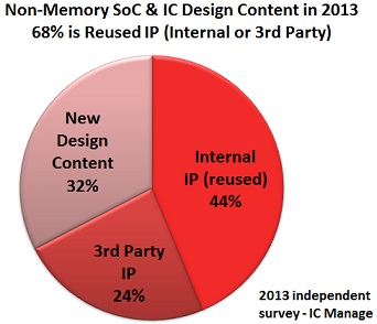 - On average, the participants expect 68 percent of their non-memory
SoC and IC design content to be reused IP.
- Further, almost 2/3rds of this reused IP will be developed internally.
So companies today are standing on the shoulders of their own giants,
leveraging their past ideas and prior implementations to rapidly
deliver each next generation of chips.
- As for the average 32% of "new" design content that's being created,
we find companies still commonly use an IP-based approach.
This IP-based approach is also true even for companies whose chips mandate
they contain mostly "new" design content.
These IP-based design approaches still require engineering groups to create
new 'IP modules' in parallel with the rest of the design -- which are still
frequently used in multiple parts of the same design. As with IP reuse, the
parallel development, integration, and assembly require ongoing team
communication, integration, and effective dependency management.
CONTINUOUS DESIGN
Why is IP reuse so prevalent?
Hardware Design is always a race. There's always been a rush to market that
goes hand-in-hand with cost, performance and low power pressures. But the
markets pressures are getting increasingly intense.
With shrinking time-to-market windows, companies don't have the luxury to
1. spec out a device,
2. design it,
3. verify it,
4. take it to market, and
5. then start work on the next design.
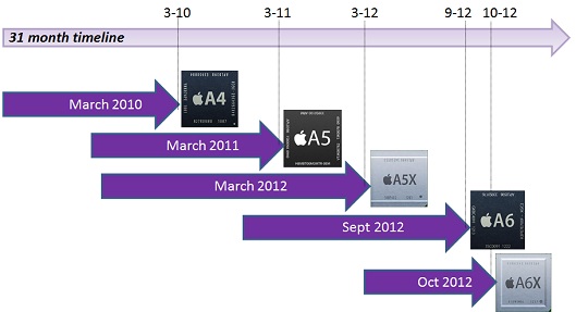
Instead engineering groups need to do continuous design. Multiple designs
are underway at any one time. Decisions are made about which version of
which modules will be included in each release. For example, Samsung
released 8 Galaxy S's in 30 months -- clearly parallel design was used to
accomplish this. Another example of continuous design is Apple. Here's
the timeline showing Apple delivering 5 processors in 31 months.
- On average, the participants expect 68 percent of their non-memory
SoC and IC design content to be reused IP.
- Further, almost 2/3rds of this reused IP will be developed internally.
So companies today are standing on the shoulders of their own giants,
leveraging their past ideas and prior implementations to rapidly
deliver each next generation of chips.
- As for the average 32% of "new" design content that's being created,
we find companies still commonly use an IP-based approach.
This IP-based approach is also true even for companies whose chips mandate
they contain mostly "new" design content.
These IP-based design approaches still require engineering groups to create
new 'IP modules' in parallel with the rest of the design -- which are still
frequently used in multiple parts of the same design. As with IP reuse, the
parallel development, integration, and assembly require ongoing team
communication, integration, and effective dependency management.
CONTINUOUS DESIGN
Why is IP reuse so prevalent?
Hardware Design is always a race. There's always been a rush to market that
goes hand-in-hand with cost, performance and low power pressures. But the
markets pressures are getting increasingly intense.
With shrinking time-to-market windows, companies don't have the luxury to
1. spec out a device,
2. design it,
3. verify it,
4. take it to market, and
5. then start work on the next design.
Instead engineering groups need to do continuous design. Multiple designs
are underway at any one time. Decisions are made about which version of
which modules will be included in each release. For example, Samsung
released 8 Galaxy S's in 30 months -- clearly parallel design was used to
accomplish this. Another example of continuous design is Apple. Here's
the timeline showing Apple delivering 5 processors in 31 months.
 In certain ways, this continuous design for hardware development mirrors the
continuous design software developers face. Software is done in releases.
The old code forms the basis for the next release. Specific new features,
enhancements, and bug fixes are targeted for each release. Hardware design
is now much more closely following this paradigm.
For both types of design (hardware and software) to win the race to market,
the teams must master IP reuse.
THE HOLY GRAIL OF IP REUSE
The holy grail of IP reuse is designers find the specific IP they need,
plug it in, and it works. In order for this to be both effective and
sustainable, the IP reuse must take less time than creating and verifying
a new design module would take. Further, the IP is usually never really
'done', and continues to evolve with use in different projects.
Below is an example of "IP-1", an internal IP that is being reused in
multiple places in the enterprise.
In certain ways, this continuous design for hardware development mirrors the
continuous design software developers face. Software is done in releases.
The old code forms the basis for the next release. Specific new features,
enhancements, and bug fixes are targeted for each release. Hardware design
is now much more closely following this paradigm.
For both types of design (hardware and software) to win the race to market,
the teams must master IP reuse.
THE HOLY GRAIL OF IP REUSE
The holy grail of IP reuse is designers find the specific IP they need,
plug it in, and it works. In order for this to be both effective and
sustainable, the IP reuse must take less time than creating and verifying
a new design module would take. Further, the IP is usually never really
'done', and continues to evolve with use in different projects.
Below is an example of "IP-1", an internal IP that is being reused in
multiple places in the enterprise.
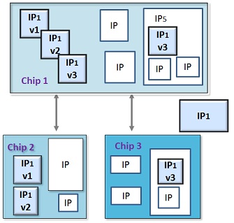 This IP might be a modem or a network processor, written at the C level or
as RTL. Notice that IP-1 has multiple instances and multiple versions,
and is being used by different design teams in multiple subsystems, designs
and design derivatives.
THE NEED TO IMPROVE
An independent survey run in Q2 2011, with 465 engineers and managers, found
that EDA verification tools (63%) and IP reuse tools (50%) were seen to be
the two top areas of SoC and IC design needing advancement over the next two
years.
This IP might be a modem or a network processor, written at the C level or
as RTL. Notice that IP-1 has multiple instances and multiple versions,
and is being used by different design teams in multiple subsystems, designs
and design derivatives.
THE NEED TO IMPROVE
An independent survey run in Q2 2011, with 465 engineers and managers, found
that EDA verification tools (63%) and IP reuse tools (50%) were seen to be
the two top areas of SoC and IC design needing advancement over the next two
years.
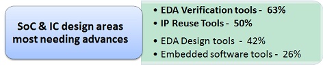 Notice how both verification and IP reuse tools even ranked above EDA design
tools (42%) and embedded software tools (26%) as needing the most help.
IP REUSE 2.0 == DESIGN REUSE + VERIFICATION REUSE
In an engineering group, enormous energy and processes can often go into
making "design reuse" happen, yet "verification reuse" is often neglected.
For efficient IP reuse across the enterprise, your company must master
BOTH the design AND the verification aspects.
- Dean Drako
IC Manage, Inc. Campbell, CA
---- ---- ---- ---- ---- ---- ----
Related Articles
And some more survey data on verification headaches and IP reuse
Dean Drako posits his design and verification IP Reuse 2.0 vision
10 design and verification "best practices" for IP Reuse 2.0 today
The Show-Me-The-Money IP Reuse 2.0 ROI and what IC Manage does
Notice how both verification and IP reuse tools even ranked above EDA design
tools (42%) and embedded software tools (26%) as needing the most help.
IP REUSE 2.0 == DESIGN REUSE + VERIFICATION REUSE
In an engineering group, enormous energy and processes can often go into
making "design reuse" happen, yet "verification reuse" is often neglected.
For efficient IP reuse across the enterprise, your company must master
BOTH the design AND the verification aspects.
- Dean Drako
IC Manage, Inc. Campbell, CA
---- ---- ---- ---- ---- ---- ----
Related Articles
And some more survey data on verification headaches and IP reuse
Dean Drako posits his design and verification IP Reuse 2.0 vision
10 design and verification "best practices" for IP Reuse 2.0 today
The Show-Me-The-Money IP Reuse 2.0 ROI and what IC Manage does
Join
Index
Next->Item
|
|


