( ESNUG 519 Item 6 ) -------------------------------------------- [02/14/13]
Subject: Berkeley CEO adds his 2 cents to Jim Hogan's Custom 2.0 Retooling
> The market pressures for gigahertz design frequencies, low cost, low
> power, and fast-yield-ramp designs are driving the move to sub-28 nm
> processes. However, while transistors are shrinking, atoms aren't.
>
> - from http://www.deepchip.com/items/0515-02.html
From: [ Ravi Subramanian of Berkeley DA ]
Hi John,
Jim pointed out some key elements, but missed a major theme in the market
drivers for Custom 2.0.
Semiconductor demand is changing big time. Companies are operating in a
world where a rapidly growing middle class will dominate silicon
consumption. According to Goldman Sachs, 170 people per minute are being
added to the middle class in the third world (China, India, Brazil, and
Africa) right now! And they now buy electronics year round, with holidays
such as Chinese New Year, Diwali and Eid.
The old model of specialty products catering to developed markets is giving
way to one platform-based design manufactured in lower cost CMOS nanometer
technologies with mass customization (high volume silicon) and localization
(programmability).
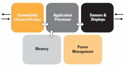
PLATFORM BASED DESIGN:
Platform-based designs consist of five main subsystems (blocks) each with
its own separately thriving ASSP businesses. These main subsystems are:
1. Connectivity (wired or wireless)
2. Application processors
3. Memory
4. Sensors
5. Power management
The complexity of these platforms is significantly greater than anything we
have seen before - Custom 2.0 verification tools must adapt to the unique
nature of each of these end applications. For example, circuit analysis for
RF connectivity applications -- often exclusively used frequency domain
analysis algorithms. However, they are implemented in bulk CMOS, resulting
in nonlinearities. Time-domain analysis algorithms perform better than
the frequency-based analysis algorithms here.
 Components of Electronic Platforms
There are also two big problems with these newer, bigger designs:
- The designs are getting MUCH more complex and they involve gluing
together high performance analog blocks right next to high
performance digital blocks on the SAME die. (Not easy to do!)
- These bigger, more complex designs at 20, 14, 10 nm will require
MUCH more complex modeling and messy silicon engineering than
ever before.
CUSTOM 2.0 AND SPICE SIMULATION:
> Even accounting for increasing the number of sim farms, SPICE simulation
> speeds need to improve 5-10x and SPICE simulation capacity needs to
> improve 100x compared with traditional SPICE simulators. Furthermore,
> both improvements must occur without giving up any accuracy.
>
> - from http://www.deepchip.com/items/0515-02.html
Jim raised some good points, but missed these two important items:
1. True mixed-signal simulation - it is not just SPICE.
As I said above, Custom 2.0 designs will be big and they'll be
far more complex than Custom 1.0 designs. For example, power
management circuits in 28 nm have dramatically different circuit
architectures that use delta-sigma modulators which never existed
in 0.18u buck-and-boost converters. These circuit architectures
have digital control, digital calibration, and digital processing
INTIMATELY working with analog building blocks to deliver key
functionality.
Another example is that all-digital PLLs are showing up everywhere.
While the voltage headroom and resolution of signals is a headache
with the move to smaller geometries, the time resolution of signals
is improving. This encourages dramatically different circuit
architectures such as time-to-digital converters, which are more
robust to operating in the 'bulk CMOS' world.
This trend towards mixed analog and digital complexity is
occurring everywhere in the platform. Jim didn't talk about the
simulation of these beasts. The headaches are formidable for AMS
engineers.
2. The emergence of "custom verification engineers".
We will know Custom 2.0 has really arrived when the role of the
"custom verification engineer" is as natural to see on a mixed
signal/custom ASSP team as it is today in the digital IC world.
Ken Kundert was the first person I know who defined and pointed
out in 2006 that such a role will necessarily emerge as the
complexity of mixed-signal systems increases.
> Just a few out of place atoms can cause severe variability in a device,
> which translates into severe variability in circuits, ultimately affecting
> the whole chip's power, performance, and yield.
>
> - from http://www.deepchip.com/items/0515-02.html
Jim noted that variation will be a big problem also. This places an
additional burden on the simulation engines.
1. Analysis algorithms must become more sophisticated than today's
traditional Fast SPICE.
The physical effects of variation, noise and layout-dependence on
electrical performance, requires that the underlying simulation
engines add new algorithms for sufficient accuracy. Traditional
fast SPICE tools like HSPICE and Spectre are limited by linearity
assumptions, single-rate analysis, and solutions to partial
differential equations. That doesn't cut it with Custom 2.0 -
what's needed here are nonlinearity, multi-rate analysis, and
stochastic differential equations. Also essential are analyses
that leverage distribution theory to identify what variation
effects ought to be analyzed.
2. Circuit Characterization across far more operating conditions.
Custom 1.0 circuit analysis was mostly ad hoc, with only a few
effects analyzed across a few corners. Due to exponential
increases in variation and complexity in sources of variation,
Custom 2.0 circuit analysis must be done systematically across
a wide range of process and operating conditions including
everything from on-die variations to the impact of operating
temperature changes in ASSPs, PMICs, and RFICs.
3. All this means that the simulation speed becomes even more
critical; at least 10x faster single-core performance is needed
so design teams can analyze more corners-per-core.
4. The selection of what to simulate needs to become much smarter -
via the use of distribution theory to define what simulations
are essential.
5. Verification against a target space of specifications.
Design and verification teams must be able to confirm the
correct operation and performance of electrical circuits across
all compliance testing conditions. What's driving this for
Custom 2.0 is:
- There are a lot more analog/mixed signal and RF blocks.
- For each block, the sheer number of tests is greater.
For example, for an nVidia Tegra or a Qualcomm Snapdragon you
might have:
- Clocking, with many different clocked domains and
clock jitter requirements.
- Power management, with multiple generated supply
voltages to service multiple types of circuitry.
- I/O blocks, with different SerDes protocols for
different I/O speeds.
To a degree, this means bringing digital verification ideas into analog
world; for example, the notion of writing a regression to test the circuit
is standard in the digital world, while still rare in the custom world.
Specifically, based on Custom 2.0 retooling at 20 and 28 nm, and BDA's
rapidly increasing R&D investment across the analog, mixed-signal, RF, and
the custom spectrum -- I'm happy to report that BDA is seeing its footprint
expand to full displacements in the custom arena.
- Ravi Subramanian
Berkeley DA Santa Clara, CA
---- ---- ---- ---- ---- ---- ----
Related Articles
Hogan outlines the history and players of the Custom 2.0 Retooling
Components of Electronic Platforms
There are also two big problems with these newer, bigger designs:
- The designs are getting MUCH more complex and they involve gluing
together high performance analog blocks right next to high
performance digital blocks on the SAME die. (Not easy to do!)
- These bigger, more complex designs at 20, 14, 10 nm will require
MUCH more complex modeling and messy silicon engineering than
ever before.
CUSTOM 2.0 AND SPICE SIMULATION:
> Even accounting for increasing the number of sim farms, SPICE simulation
> speeds need to improve 5-10x and SPICE simulation capacity needs to
> improve 100x compared with traditional SPICE simulators. Furthermore,
> both improvements must occur without giving up any accuracy.
>
> - from http://www.deepchip.com/items/0515-02.html
Jim raised some good points, but missed these two important items:
1. True mixed-signal simulation - it is not just SPICE.
As I said above, Custom 2.0 designs will be big and they'll be
far more complex than Custom 1.0 designs. For example, power
management circuits in 28 nm have dramatically different circuit
architectures that use delta-sigma modulators which never existed
in 0.18u buck-and-boost converters. These circuit architectures
have digital control, digital calibration, and digital processing
INTIMATELY working with analog building blocks to deliver key
functionality.
Another example is that all-digital PLLs are showing up everywhere.
While the voltage headroom and resolution of signals is a headache
with the move to smaller geometries, the time resolution of signals
is improving. This encourages dramatically different circuit
architectures such as time-to-digital converters, which are more
robust to operating in the 'bulk CMOS' world.
This trend towards mixed analog and digital complexity is
occurring everywhere in the platform. Jim didn't talk about the
simulation of these beasts. The headaches are formidable for AMS
engineers.
2. The emergence of "custom verification engineers".
We will know Custom 2.0 has really arrived when the role of the
"custom verification engineer" is as natural to see on a mixed
signal/custom ASSP team as it is today in the digital IC world.
Ken Kundert was the first person I know who defined and pointed
out in 2006 that such a role will necessarily emerge as the
complexity of mixed-signal systems increases.
> Just a few out of place atoms can cause severe variability in a device,
> which translates into severe variability in circuits, ultimately affecting
> the whole chip's power, performance, and yield.
>
> - from http://www.deepchip.com/items/0515-02.html
Jim noted that variation will be a big problem also. This places an
additional burden on the simulation engines.
1. Analysis algorithms must become more sophisticated than today's
traditional Fast SPICE.
The physical effects of variation, noise and layout-dependence on
electrical performance, requires that the underlying simulation
engines add new algorithms for sufficient accuracy. Traditional
fast SPICE tools like HSPICE and Spectre are limited by linearity
assumptions, single-rate analysis, and solutions to partial
differential equations. That doesn't cut it with Custom 2.0 -
what's needed here are nonlinearity, multi-rate analysis, and
stochastic differential equations. Also essential are analyses
that leverage distribution theory to identify what variation
effects ought to be analyzed.
2. Circuit Characterization across far more operating conditions.
Custom 1.0 circuit analysis was mostly ad hoc, with only a few
effects analyzed across a few corners. Due to exponential
increases in variation and complexity in sources of variation,
Custom 2.0 circuit analysis must be done systematically across
a wide range of process and operating conditions including
everything from on-die variations to the impact of operating
temperature changes in ASSPs, PMICs, and RFICs.
3. All this means that the simulation speed becomes even more
critical; at least 10x faster single-core performance is needed
so design teams can analyze more corners-per-core.
4. The selection of what to simulate needs to become much smarter -
via the use of distribution theory to define what simulations
are essential.
5. Verification against a target space of specifications.
Design and verification teams must be able to confirm the
correct operation and performance of electrical circuits across
all compliance testing conditions. What's driving this for
Custom 2.0 is:
- There are a lot more analog/mixed signal and RF blocks.
- For each block, the sheer number of tests is greater.
For example, for an nVidia Tegra or a Qualcomm Snapdragon you
might have:
- Clocking, with many different clocked domains and
clock jitter requirements.
- Power management, with multiple generated supply
voltages to service multiple types of circuitry.
- I/O blocks, with different SerDes protocols for
different I/O speeds.
To a degree, this means bringing digital verification ideas into analog
world; for example, the notion of writing a regression to test the circuit
is standard in the digital world, while still rare in the custom world.
Specifically, based on Custom 2.0 retooling at 20 and 28 nm, and BDA's
rapidly increasing R&D investment across the analog, mixed-signal, RF, and
the custom spectrum -- I'm happy to report that BDA is seeing its footprint
expand to full displacements in the custom arena.
- Ravi Subramanian
Berkeley DA Santa Clara, CA
---- ---- ---- ---- ---- ---- ----
Related Articles
Hogan outlines the history and players of the Custom 2.0 Retooling
Join
Index
Next->Item
|
|