( ESNUG 515 Item 5 ) -------------------------------------------- [11/29/12]
From: [ Jim Hogan of Vista Ventures LLC ]
Subject: 3D FinFETs mean lots and lots of SPICE runs even with Custom 2.0
Hi, John,
A FinFET transistor is a 3D structure that rises above the planar substrate
(Figure 8). The result is that the structure has noticably more volume than
a planar gate for the same planar area.
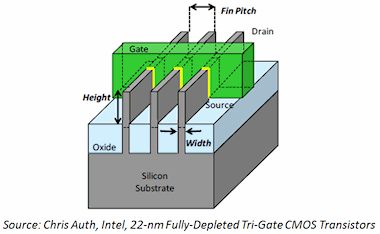 Figure 8: FinFET transistor
Because the gate wraps around the channel, the structure is far more complex
than a planar transistor. The manufacturing challenges are considerable.
Intel has certainly led the world in this capability. It's not clear to me
at least who will be able to stay in the foundry game going forward.
A FinFET transistor has the advantage of much lower leakage current, but
results in significantly more complexity both in manufacturing and design.
The complementary "3D" technology to help reduce leakage is FD-SOI (fully
depleted silicon-on-insulator).
EDA TOOLS AND FINFETS
Modeling 3D FinFETS is a mixed bag. FinFETs are not as affected by leakage,
so one does not need to model those issues as accurately. However, higher
model complexity is required due to the 3D nature of FinFET devices. The
multiple fins making up the 3D transistors introduce a large number of new
parasitic resistances and capacitances -- that have to all be considered in
extraction, modeling, and simulation.
Another problem is device and circuit engineers don't have the decades of
experience and rules-of-thumb that they have with 2D (planar) devices.
Furthermore, new information is needed to develop models for source/drain
resistance extensions, contact resistances, fringing effects and the wider
number of coupling capacitances introduced by the 3D structures. This
means far more equations are needed to represent a single FinFET transistor
compared to a planar transistor.
These have all been standardized in the BSIM-CMG (Berkeley Short-channel
IGFET Model for Common Multi-Gate) compact model and are used by BDA's
Analog FastSPICE, Cadence's Spectre, and Synopsys' HSPICE simulators
to validate circuit designs.
Figure 8: FinFET transistor
Because the gate wraps around the channel, the structure is far more complex
than a planar transistor. The manufacturing challenges are considerable.
Intel has certainly led the world in this capability. It's not clear to me
at least who will be able to stay in the foundry game going forward.
A FinFET transistor has the advantage of much lower leakage current, but
results in significantly more complexity both in manufacturing and design.
The complementary "3D" technology to help reduce leakage is FD-SOI (fully
depleted silicon-on-insulator).
EDA TOOLS AND FINFETS
Modeling 3D FinFETS is a mixed bag. FinFETs are not as affected by leakage,
so one does not need to model those issues as accurately. However, higher
model complexity is required due to the 3D nature of FinFET devices. The
multiple fins making up the 3D transistors introduce a large number of new
parasitic resistances and capacitances -- that have to all be considered in
extraction, modeling, and simulation.
Another problem is device and circuit engineers don't have the decades of
experience and rules-of-thumb that they have with 2D (planar) devices.
Furthermore, new information is needed to develop models for source/drain
resistance extensions, contact resistances, fringing effects and the wider
number of coupling capacitances introduced by the 3D structures. This
means far more equations are needed to represent a single FinFET transistor
compared to a planar transistor.
These have all been standardized in the BSIM-CMG (Berkeley Short-channel
IGFET Model for Common Multi-Gate) compact model and are used by BDA's
Analog FastSPICE, Cadence's Spectre, and Synopsys' HSPICE simulators
to validate circuit designs.
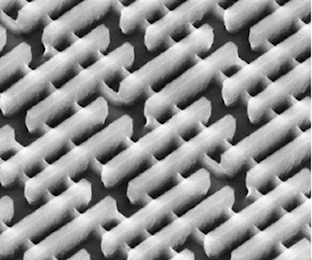 Figure 9: Intel 22 nm trigate FinFET
Clearly 3D FinFETs will be the prominent technology in the coming decade,
impacting logic and memory design. In 2012, we had Intel's trigate FinFET
at 22 nm (Figure 9). In 2014, we will have ultra-thin body, fully depleted
SOIs at 14 nm.
- Jim Hogan
Vista Ventures, LLC Los Gatos, CA
---- ---- ---- ---- ---- ---- ----
Related Articles
Hogan on the early days of Custom 1.0 and Cadence Analog Artist
Key aspects, market drivers for the present Custom 2.0 retooling
Atomic scaling problems, Variation, and the Custom 2.0 retooling
Custom 2.0 means that SPICE runs must BOTH be fast AND accurate
Custom 2.0 is design data dependencies, NOT design data managment
Hogan outlines the current players for the Custom 2.0 retooling
Figure 9: Intel 22 nm trigate FinFET
Clearly 3D FinFETs will be the prominent technology in the coming decade,
impacting logic and memory design. In 2012, we had Intel's trigate FinFET
at 22 nm (Figure 9). In 2014, we will have ultra-thin body, fully depleted
SOIs at 14 nm.
- Jim Hogan
Vista Ventures, LLC Los Gatos, CA
---- ---- ---- ---- ---- ---- ----
Related Articles
Hogan on the early days of Custom 1.0 and Cadence Analog Artist
Key aspects, market drivers for the present Custom 2.0 retooling
Atomic scaling problems, Variation, and the Custom 2.0 retooling
Custom 2.0 means that SPICE runs must BOTH be fast AND accurate
Custom 2.0 is design data dependencies, NOT design data managment
Hogan outlines the current players for the Custom 2.0 retooling
Join
Index
Next->Item
|
|


