( ESNUG 515 Item 3 ) -------------------------------------------- [11/29/12]
From: [ Jim Hogan of Vista Ventures LLC ]
Subject: Atomic scaling problems, Variation, and the Custom 2.0 retooling
Hi, John,
Moore's Law continues to march on. Devices are shrinking, and will continue
to shrink for the foreseeable future. However, while transistors keep
shrinking, atoms do not.
Custom 1.0 devices, as shown on the left in Figure 3 below, used to have
Avogadro-size atom counts (10^23 and above). As such, a few atoms out of
place due to random dopant fluctuations or other process variations did not
have a major impact on device performance.
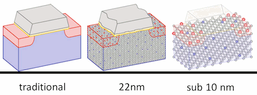 Figure 3: Atomic-level variation effects with shrinking processes
In contrast, Custom 2.0 design problems are atomic in scale. At 20 nm, we
can basically count the atoms: 20 nm is 200 angstroms, meaning only 200
hydrogen atoms or 80 copper atoms wide. So small fluctuations now have
critical impact on process variability.
For example, typically the oxide layer of a gate is just a few atoms thick,
and even one single out of place atom can change device performance
considerably. One atom! As a result, Moore's Law is flattening out for
performance and power; we can no longer expect the same scaling we've had
for so long.
INDIVIDUAL ATOMS
Figure 4 below shows another example of what occurs when each individual
atom starts to have more of an effect.
Figure 3: Atomic-level variation effects with shrinking processes
In contrast, Custom 2.0 design problems are atomic in scale. At 20 nm, we
can basically count the atoms: 20 nm is 200 angstroms, meaning only 200
hydrogen atoms or 80 copper atoms wide. So small fluctuations now have
critical impact on process variability.
For example, typically the oxide layer of a gate is just a few atoms thick,
and even one single out of place atom can change device performance
considerably. One atom! As a result, Moore's Law is flattening out for
performance and power; we can no longer expect the same scaling we've had
for so long.
INDIVIDUAL ATOMS
Figure 4 below shows another example of what occurs when each individual
atom starts to have more of an effect.
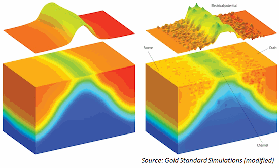 Figure 4: Device-level electrical potential before
and now (under variation)
In this case we are looking at how electrical potential varies on a device.
The left side is a traditional or ideal device, where there are so many
atoms that electrical potential looks "smoothed out". The right side shows
more recent devices, where individual atoms cause roughness everywhere.
This is due to random fluctuations in the dopant atoms' locations and
concentrations. This roughness affects device electrical potential, and in
turn, device performance. From an EDA tool perspective, this presents both
modeling and algorithmic problems.
To better assess the effect of the roughness on device performance, Figure 5
looks at performance in terms of threshold voltage.
Figure 4: Device-level electrical potential before
and now (under variation)
In this case we are looking at how electrical potential varies on a device.
The left side is a traditional or ideal device, where there are so many
atoms that electrical potential looks "smoothed out". The right side shows
more recent devices, where individual atoms cause roughness everywhere.
This is due to random fluctuations in the dopant atoms' locations and
concentrations. This roughness affects device electrical potential, and in
turn, device performance. From an EDA tool perspective, this presents both
modeling and algorithmic problems.
To better assess the effect of the roughness on device performance, Figure 5
looks at performance in terms of threshold voltage.
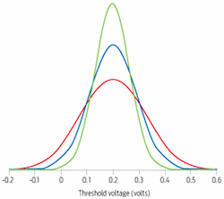 Figure 5: Custom 2.0 design variation: widening threshold voltage
This is important because it is this ability that allows us to have the
illusion of a binary switch. Threshold voltage ideally varies as little as
possible from device to device. However, as we move to smaller geometries,
threshold voltage has increasingly larger variance; this larger variance in
device performance translates to more variance in circuit performance, with
a resulting yield loss and missed power budgets.
When we combine the shrinking transistors with the fixed atom sizes for
Custom 2.0 designs, even a few random dopant atoms out of place can actually
affect transistor performance. At the extreme, we can even have negative
threshold voltages - the transistors no longer operate as switches. Such
high device performance variability can make a circuit's performance
unacceptably unpredictable.
TRADITIONAL VARIATION MANAGEMENT
In traditional design flows, designers would design against the fast-fast
(FF) and slow-slow (SS) process corners of the distribution supplied by the
foundry -- and maybe other similar corners -- in order to manage variation.
The FF and SS corners could bracket a circuit's performance, so the designer
could account for the bounds of performance across process variation.
However, Figure 6 shows an example of the relationship between FF and SS
corners and the true distribution for a 28 nm design, clearly showing that
the SS and FF corners no longer capture the bounds of the distribution.
Figure 5: Custom 2.0 design variation: widening threshold voltage
This is important because it is this ability that allows us to have the
illusion of a binary switch. Threshold voltage ideally varies as little as
possible from device to device. However, as we move to smaller geometries,
threshold voltage has increasingly larger variance; this larger variance in
device performance translates to more variance in circuit performance, with
a resulting yield loss and missed power budgets.
When we combine the shrinking transistors with the fixed atom sizes for
Custom 2.0 designs, even a few random dopant atoms out of place can actually
affect transistor performance. At the extreme, we can even have negative
threshold voltages - the transistors no longer operate as switches. Such
high device performance variability can make a circuit's performance
unacceptably unpredictable.
TRADITIONAL VARIATION MANAGEMENT
In traditional design flows, designers would design against the fast-fast
(FF) and slow-slow (SS) process corners of the distribution supplied by the
foundry -- and maybe other similar corners -- in order to manage variation.
The FF and SS corners could bracket a circuit's performance, so the designer
could account for the bounds of performance across process variation.
However, Figure 6 shows an example of the relationship between FF and SS
corners and the true distribution for a 28 nm design, clearly showing that
the SS and FF corners no longer capture the bounds of the distribution.
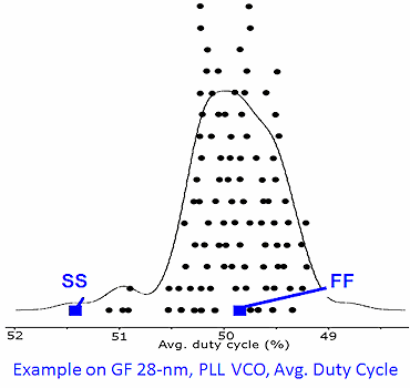 Figure 6: Custom 2.0: FF/SS corners no longer applicable
In particular, FF is very far off, so there is nothing to capture the upper
bound of the distribution.
There are two reasons for the disparity. First, FF and SS corners are
designed to bracket performance at the device level for the digital
performance measures of speed and power. They do not handle arbitrary
analog performance outputs, such as duty cycle. Second, FF and SS corners
only model global variation; they ignore local (mismatch) variation.
Mismatch used to have a 5% effect and now it can have up to a 50% effect.
When we account for local variation in medium- and large- sized circuits, we
are looking at thousands or even tens of thousands of process variables.
CUSTOM 2.0 VARIATION MANAGEMENT
For Custom 2.0, this means that traditional digital FF/SS corners will no
longer suffice. We need tools that handle statistical process variation
quickly, accurately, reliably, and at scale to industrially-sized circuits
comprising thousands of elements or more. Inside the design loop, Monte
Carlo is too slow; we need "true" analog 3-sigma corners for each analog
performance output, as a function of both global and local process
variation, and therefore specific to the circuit being designed.
Further, we need a fast way to verify designs under process variation, to
a high statistical confidence.
Extreme process variation impacts more than just analog circuits such as the
VCO above. Extreme process variation has an even bigger effect on circuits
where an extremely high yield is a must-have. Such high-sigma circuits
include:
- Highly replicated blocks, such as bitcells, sense amps, and
std cells must be high sigma, so that when many of them are
put into an overall chip, the overall yield of the chip can hit
2-3 sigma (95%-99.73%). As an example, if you had 10 blocks and
each had a 90% chance of working, then the chip with 10 blocks
would have a yield of 95% * 95% * ... 95% = 0.95^10, or 60.0%.
That's abysmal. Now imagine if you have a million blocks, such as
a 1 Mbit memory. Each block had better be extremely reliable.
- Circuits where failure is disastrous. In a DAC 2012 panel session
on reliability, Sani Nassif gave a compelling criterion: "Would
you put this device in your heart?" You really want that 1 in a
million (or 1 in a billion) chance of failure for medical devices,
airplanes, automobiles, etc. These are application that are not
just mission-critical but life-critical.
As for designing a high-sigma circuit to handle such variation effects, we
cannot run 1000's of simulations every design change, let alone 5 billion.
For example:
- Verifying under PVT conditions was historically done with 10-100
PVT corners, as combinations of FF/SS/TT, temperature, and load.
However, modeling the effect of double patterning lithography
requires special parasitics; this increases the total PVT corner
count by 15x to 20x, to approximately 2,000 corners.
- Verifying a 3-sigma design (yield of 99.86%) with a high degree of
confidence takes up to 5,000 Monte Carlo samples. For a circuit
that takes 30 seconds for a single simulation, simulating 5,000
Monte Carlo samples would take 42 hours on a single core.
- Verifying a 6-sigma design takes about 5,000,000,000 Monte Carlo
samples. If the circuit takes only 1 second to simulate,
simulating all 5,000,000,000 samples would take 159 years.
The number of simulations required for variation analysis must come down by
multiple orders of magnitude.
As Chairman of the Solido board, I've spend a lot of time investigating
this SPICE analysis and variation problem deeply.
- Jim Hogan
Vista Ventures, LLC Los Gatos, CA
---- ---- ---- ---- ---- ---- ----
Related Articles
Hogan on the early days of Custom 1.0 and Cadence Analog Artist
Key aspects, market drivers for the present Custom 2.0 retooling
Custom 2.0 means that SPICE runs must BOTH be fast AND accurate
3D FinFETs mean lots and lots of SPICE runs even with Custom 2.0
Custom 2.0 is design data dependencies, NOT design data managment
Hogan outlines the current players for the Custom 2.0 retooling
Figure 6: Custom 2.0: FF/SS corners no longer applicable
In particular, FF is very far off, so there is nothing to capture the upper
bound of the distribution.
There are two reasons for the disparity. First, FF and SS corners are
designed to bracket performance at the device level for the digital
performance measures of speed and power. They do not handle arbitrary
analog performance outputs, such as duty cycle. Second, FF and SS corners
only model global variation; they ignore local (mismatch) variation.
Mismatch used to have a 5% effect and now it can have up to a 50% effect.
When we account for local variation in medium- and large- sized circuits, we
are looking at thousands or even tens of thousands of process variables.
CUSTOM 2.0 VARIATION MANAGEMENT
For Custom 2.0, this means that traditional digital FF/SS corners will no
longer suffice. We need tools that handle statistical process variation
quickly, accurately, reliably, and at scale to industrially-sized circuits
comprising thousands of elements or more. Inside the design loop, Monte
Carlo is too slow; we need "true" analog 3-sigma corners for each analog
performance output, as a function of both global and local process
variation, and therefore specific to the circuit being designed.
Further, we need a fast way to verify designs under process variation, to
a high statistical confidence.
Extreme process variation impacts more than just analog circuits such as the
VCO above. Extreme process variation has an even bigger effect on circuits
where an extremely high yield is a must-have. Such high-sigma circuits
include:
- Highly replicated blocks, such as bitcells, sense amps, and
std cells must be high sigma, so that when many of them are
put into an overall chip, the overall yield of the chip can hit
2-3 sigma (95%-99.73%). As an example, if you had 10 blocks and
each had a 90% chance of working, then the chip with 10 blocks
would have a yield of 95% * 95% * ... 95% = 0.95^10, or 60.0%.
That's abysmal. Now imagine if you have a million blocks, such as
a 1 Mbit memory. Each block had better be extremely reliable.
- Circuits where failure is disastrous. In a DAC 2012 panel session
on reliability, Sani Nassif gave a compelling criterion: "Would
you put this device in your heart?" You really want that 1 in a
million (or 1 in a billion) chance of failure for medical devices,
airplanes, automobiles, etc. These are application that are not
just mission-critical but life-critical.
As for designing a high-sigma circuit to handle such variation effects, we
cannot run 1000's of simulations every design change, let alone 5 billion.
For example:
- Verifying under PVT conditions was historically done with 10-100
PVT corners, as combinations of FF/SS/TT, temperature, and load.
However, modeling the effect of double patterning lithography
requires special parasitics; this increases the total PVT corner
count by 15x to 20x, to approximately 2,000 corners.
- Verifying a 3-sigma design (yield of 99.86%) with a high degree of
confidence takes up to 5,000 Monte Carlo samples. For a circuit
that takes 30 seconds for a single simulation, simulating 5,000
Monte Carlo samples would take 42 hours on a single core.
- Verifying a 6-sigma design takes about 5,000,000,000 Monte Carlo
samples. If the circuit takes only 1 second to simulate,
simulating all 5,000,000,000 samples would take 159 years.
The number of simulations required for variation analysis must come down by
multiple orders of magnitude.
As Chairman of the Solido board, I've spend a lot of time investigating
this SPICE analysis and variation problem deeply.
- Jim Hogan
Vista Ventures, LLC Los Gatos, CA
---- ---- ---- ---- ---- ---- ----
Related Articles
Hogan on the early days of Custom 1.0 and Cadence Analog Artist
Key aspects, market drivers for the present Custom 2.0 retooling
Custom 2.0 means that SPICE runs must BOTH be fast AND accurate
3D FinFETs mean lots and lots of SPICE runs even with Custom 2.0
Custom 2.0 is design data dependencies, NOT design data managment
Hogan outlines the current players for the Custom 2.0 retooling
Join
Index
Next->Item
|
|


