!!! "It's not a BUG,  /o o\ / it's a FEATURE!" (508) 429-4357
( > )
\ - / INDUSTRY GADFLY: "Graham's Synopsys-Verdi Interop Trip Report"
_] [_
by John Cooley
Holliston Poor Farm, P.O. Box 6222, Holliston, MA 01746-6222
---- ---- ---- ---- ---- ---- ----
Hi, John,
Here's my trip report for the Synopsys-Verdi Interoperability Forum
that was held inside the San Jose SNUG'14.
- Graham Bell
Real Intent, Inc. Sunnyvale, CA
---- ---- ---- ---- ---- ---- ----
VIA'14 ATTENDANCE NUMBERS
The VIA'14 conference was held at SNUG Silicon Valley, Wednesday, March 26,
2014 from 3 - 7 PM at the Santa Clara Convention Center in rooms 203/204.
The room was full. I estimate the attendance at 150-200 people.
---- ---- ---- ---- ---- ---- ----
The event was hosted by Dave DeMaria, VP of Verification Marketing at SNPS.
Dave started right off with a slide that declared the "Synopsys Commitment"
to:
- Verdi 3 being Open and Interoperable with Third-Party Tools
- Continuing Open Support of ALL major simulators, emulators
and formal engines
I didn't catch if Dave listed the specific 3rd-party tools that he claimed
Synopsys was committed to supporting.
---- ---- ---- ---- ---- ---- ----
Next came YuChin Hsu, VP of Verification R&D at Synopsys. He said "VIA is
Verdi's baby" and then YuChin described how Verdi has both C-based API and
TCL interfaces.
YuChin presented this diagram:
/o o\ / it's a FEATURE!" (508) 429-4357
( > )
\ - / INDUSTRY GADFLY: "Graham's Synopsys-Verdi Interop Trip Report"
_] [_
by John Cooley
Holliston Poor Farm, P.O. Box 6222, Holliston, MA 01746-6222
---- ---- ---- ---- ---- ---- ----
Hi, John,
Here's my trip report for the Synopsys-Verdi Interoperability Forum
that was held inside the San Jose SNUG'14.
- Graham Bell
Real Intent, Inc. Sunnyvale, CA
---- ---- ---- ---- ---- ---- ----
VIA'14 ATTENDANCE NUMBERS
The VIA'14 conference was held at SNUG Silicon Valley, Wednesday, March 26,
2014 from 3 - 7 PM at the Santa Clara Convention Center in rooms 203/204.
The room was full. I estimate the attendance at 150-200 people.
---- ---- ---- ---- ---- ---- ----
The event was hosted by Dave DeMaria, VP of Verification Marketing at SNPS.
Dave started right off with a slide that declared the "Synopsys Commitment"
to:
- Verdi 3 being Open and Interoperable with Third-Party Tools
- Continuing Open Support of ALL major simulators, emulators
and formal engines
I didn't catch if Dave listed the specific 3rd-party tools that he claimed
Synopsys was committed to supporting.
---- ---- ---- ---- ---- ---- ----
Next came YuChin Hsu, VP of Verification R&D at Synopsys. He said "VIA is
Verdi's baby" and then YuChin described how Verdi has both C-based API and
TCL interfaces.
YuChin presented this diagram:
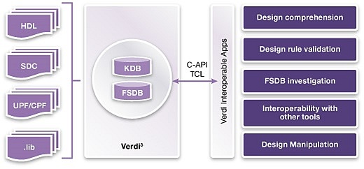 and discussed how the Verdi 3 parser, netlist and simulation db's support
the "Apps from Design Comprehension through Design Manipulation".
The intent here is to write little Verdi 3 apps that are valuable to the
design and verification engineers but the EDA vendor does not provide.
The basic idea is to create a push button in your CAD reporting tool that
will launch Verdi for debug.
There are 60+ pre-loaded Verdi 3 apps (with source in C/TCL) that come
with the Verdi distribution. The VIA-Exchange web-site is available for
the free sharing of apps to the design community at large, with videos
and other document resources online.
---- ---- ---- ---- ---- ---- ----
JIM HOGAN'S KEYNOTE ADDRESS
Dave DeMaria introduced Jim Hogan as his mentor from his time at Cadence.
Jim corrected Dave and said "I was your tormentor".
Jim's message was how API's accelerate discovery and innovation -- and
lower the barrier to accessing information.
Jim started with how the internet evolved from Web 2.0, "the social web",
to Web 3.0, "the semantic web", and next we are going to see:
"Web 4.0 -- which is everywhere, all the time, and that talks
back to you and maybe even thinks for you, too."
The glue to making all this work is getting access to the data.
What about traditional software standard activities? Traditional SW
standards:
- can easily take 10 years (e.g. Verilog) to create;
- are usually driven by vendors, and
- the consumers are locked out;
- only provides lowest-common denominator features
(e.g. "you get size 9 brown shoes only"), and
- innovation is glacial.
Conversely, the modern growth of Open API's has been exponential.
and discussed how the Verdi 3 parser, netlist and simulation db's support
the "Apps from Design Comprehension through Design Manipulation".
The intent here is to write little Verdi 3 apps that are valuable to the
design and verification engineers but the EDA vendor does not provide.
The basic idea is to create a push button in your CAD reporting tool that
will launch Verdi for debug.
There are 60+ pre-loaded Verdi 3 apps (with source in C/TCL) that come
with the Verdi distribution. The VIA-Exchange web-site is available for
the free sharing of apps to the design community at large, with videos
and other document resources online.
---- ---- ---- ---- ---- ---- ----
JIM HOGAN'S KEYNOTE ADDRESS
Dave DeMaria introduced Jim Hogan as his mentor from his time at Cadence.
Jim corrected Dave and said "I was your tormentor".
Jim's message was how API's accelerate discovery and innovation -- and
lower the barrier to accessing information.
Jim started with how the internet evolved from Web 2.0, "the social web",
to Web 3.0, "the semantic web", and next we are going to see:
"Web 4.0 -- which is everywhere, all the time, and that talks
back to you and maybe even thinks for you, too."
The glue to making all this work is getting access to the data.
What about traditional software standard activities? Traditional SW
standards:
- can easily take 10 years (e.g. Verilog) to create;
- are usually driven by vendors, and
- the consumers are locked out;
- only provides lowest-common denominator features
(e.g. "you get size 9 brown shoes only"), and
- innovation is glacial.
Conversely, the modern growth of Open API's has been exponential.
 In general, closed integrations are like the rings of Saturn -- "you can't
escape their orbit once you are locked in," said Jim.
Now that companies have access to the data, they can add their intelligence
to produce the analytics needed for Web 3.0.
Jim Hogan isn't an anarchist.
He pointed out that an API needed governance. This means an organization
that:
- manages the overall project,
- has admin support, leadership, represents key stakeholders,
- has development and management tools,
- has people to run the project, and,
- finally a way to enforce and manage quality control.
Jim Hogan then returned to stress the need for an Open API by pointing out
Chris Anderson's TED talks on Crowd Accelerated Innovation that have been
around since 1987. Chris points out three ingredients for innovation:
- Technology
- Interest in an existing successful (big enough) ecosystem
- Light: visibility of what is possible.
Jim then proclaimed that Verdi 3 plus VIA had these elements.
Jim Hogan likes to make money from innovation. In his keynot, Jim presented
his famous Design Tool Meta Model slide, showing where the money is in the
EDA world:
In general, closed integrations are like the rings of Saturn -- "you can't
escape their orbit once you are locked in," said Jim.
Now that companies have access to the data, they can add their intelligence
to produce the analytics needed for Web 3.0.
Jim Hogan isn't an anarchist.
He pointed out that an API needed governance. This means an organization
that:
- manages the overall project,
- has admin support, leadership, represents key stakeholders,
- has development and management tools,
- has people to run the project, and,
- finally a way to enforce and manage quality control.
Jim Hogan then returned to stress the need for an Open API by pointing out
Chris Anderson's TED talks on Crowd Accelerated Innovation that have been
around since 1987. Chris points out three ingredients for innovation:
- Technology
- Interest in an existing successful (big enough) ecosystem
- Light: visibility of what is possible.
Jim then proclaimed that Verdi 3 plus VIA had these elements.
Jim Hogan likes to make money from innovation. In his keynot, Jim presented
his famous Design Tool Meta Model slide, showing where the money is in the
EDA world:
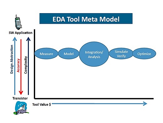 The more an EDA tool analyzes, verifies, and optimizes; the more valuable it
will be to paying customers.
Jim concluded his talk by discussing how end users now value what's in
the system instead of in the device. He used the example of the FitBit
wrist monitor for your physical activity.
The more an EDA tool analyzes, verifies, and optimizes; the more valuable it
will be to paying customers.
Jim concluded his talk by discussing how end users now value what's in
the system instead of in the device. He used the example of the FitBit
wrist monitor for your physical activity.
 FitBit talks to your smartphone (your hub) and all data that is collected is
stored in the Cloud, with ready access anywhere. In the Cloud is where the
big data analytics happen (by your insurance company?!)
GRAHAM'S ANALYSIS OF JIM'S KEYNOTE
My take on Open API's is that they are great for creating dedicated apps,
but are not as general purpose as the script-ware that EDA professionals
are familiar with.
Text-based scripts can easily be adjusted to match shifting requirements
of a design flow, and text scripts can overcome the "mismatches" between
different EDA vendors' tools.
With that said, one API that has become a standard in EDA is the Verilog
Procedural Interface (VPI), originally known as PLI 2.0, -- and is part
of the IEEE 1364 standard. It allows behavioral Verilog code to invoke
C functions, and C functions to invoke standard Verilog system tasks.
Test harnesses, instruction set simulators, and debuggers are some of the
uses for the VPI API.
VPI delivers the high-performance and tight integration needed for such
dedicated applications, but the VPI suffers from the burden of programming
and associated debug/maintenance issues.
Despite Jim Hogan's prediction, I believe script-aware will remain the
dominant mode of EDA tool integration since it is very easy to maintain
and gives good enough performance for most tasks. I don't think "make"
files will go away any time in the near future for EDA users.
---- ---- ---- ---- ---- ---- ----
---- ---- ---- ---- ---- ---- ----
---- ---- ---- ---- ---- ---- ----
USER PAPER: Innovation and the Debug Challenge
by Tony Chen, Dir of Eng at Qualcomm QTI, San Diego, CA
Tony opened by saying he was here to echo the problems he sees at QTI and
to affirm the need for openness and support for his Design Automation team;
and to lower the cost of design and debug.
QTI is the chip division of Qualcomm and it sells SnapDragon processors
that are in 1350+ phones, and 40+ tablets.
To continue to be successful, Tony said his engineers need to do more chips,
but they must shrink development time to months -- and the development cost
needs to be LOW to meet the requirements of Tier 2 and Tier 3 customers.
Tony went on to describe QTI as a mobile baseband leader that supports many
standards, and uses 20 nm and below silicon to implement chips with billions
of transistors. He characterized their designs as "a kind of personal
computer with new multimedia graphic capability." The growing complexity
QTI faces in verification include:
- Number of tests
- Number of coverage bins
- Multi-tier verification
- System-level implication
He then specifically outlined the scope of SoC Verification at QTI
- Integration of IP memory, processor, modem, multimedia, peripherals
- Clock verification
- Interconnect architecture verification
- Use case interaction
- Power intent verification
- Low power techniques in simulation and debug
- System-level security
The performance of your final SOC needs to be seen early on, so end-to-end
verification has to be done to make sure the chip runs fast enough.
Verification is executed at various levels of abstraction from core and
sub-system up to the SOC and system/architecture levels. The flow and
methodology include:
- SOC test plan and coverage
- Simulation
- Formal verification
- Power aware
- HW/SW co-verification
Tony reiterated the old cliche that verification is largest part of a chip
budget, and showed a slide with 10-year-old data where verification and
debug was 35-50% of the design cycle. He went on to say that in his
experience this has gotten worse.
Not surprisingly he said more innovation is needed. He saw four trends:
- HW-based verification is mainstream.
- Early software development is a MUST.
- Need for a hybrid verification environment working across
virtual, simulation and emulation platforms.
- RTL and gate-level SW verification still necessary.
Tony summarized by reiterating Qualcomm has a heterogeneous environment, so
open interface support is key to their bringing all the pieces together.
---- ---- ---- ---- ---- ---- ----
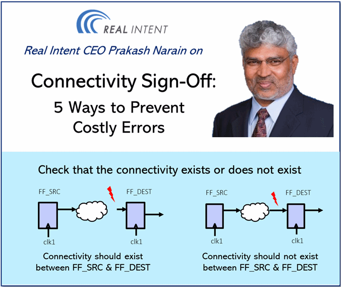
USER PAPER: Connectivity Verification using the VIA NPI
by Ariel More, Verification Engineer at Intel, Haifa, Israel
Ariel focuses on analog-mixed/signal (AMS) verification in Intel's
designs. One key issue is mishaps at the interface between analog
and digital components. His specific concern is the connectivity of
analog power gates that are part of the control path for a design.
(The power agents across the chip and control paths must be direct;
and not be mistakenly routed through digital gates.)
Previously, Intel did a visual review of their design with Verdi, but
this manual approach does not scale. The safest method for correctness
is a simulation of both digital and analog sides of the interface.
However the runtimes involved is prohibitive.
Instead design instance checkers that look at all ports -- and checks
their drivers and loads -- can be written in Verdi's TCL language.
The Verdi GUI operations are echoed in a TCL view for easy copying into
scripts which are written for automated checks. Ariel presented example
code derived for the Novas Programmable Interface (NPI). Ariel went on
to explain that since knowledge of the connectivity can be derived from
the Verdi design database (KDB), checkers can be written in Perl to look
for problems. Depending on the verification requirements, the Perl
checkers can be fine-tuned as needed.
The upside to the VIA checker approach:
- Checking is automatic. It's not manual, which is
error-prone and slow.
- Runtimes are minutes, and can be done offline on
the KDB design database.
- Checkers are robust; they check all design changes.
The one downside is that this is not "true" functional testing (i.e.
simulation) of the design. It's only as good as the checkers are.
Ariel concluded by describing Intel's future plans for coverage of very
distant (deeper) dependencies, and power checks.
---- ---- ---- ---- ---- ---- ----
USER PAPER: VIA for In-house Design Rule Checking
by Pine Yan, Sr. DFT Manager at Nvidia, Santa Clara, CA
Pine opened his talk by sharing how Nvidia does many different kinds of
design-rule checking (DRC) for logic functions, clocking, timing, power,
and DFT. These checks work at both RTL- and gate-level, and are used by
multiple teams.
Their initial debug environment was command line interface (CLI)-based
and had a deep learning curve. It had a VIM or EMACS (text-based) debug
approach that was primitive and had individual checkers that did not scale.
In addition, synchronization between the RT-level and gate-level was hard
to do.
They wanted a GUI which associated their design in context to its error
report. Ideally, it would let them jump from an error report directly to
the specific design nodes concerned. They couldn't find any off-the-shelf
DRC tools that could do this until Verdi 3.
Verdi customization allowed new menu items for a Nvidia-specific flow, with
schematic annotation of checkers. Its GUI has a TCL-based interface.
The Nvidia DRC tool generates an error report -- and the Nvidia Design
Evaluator tool has a TCL socket into Verdi. Verdi's CMD window can also
talk back to the Design Evaluator, so two-way communication is supported.
For each kind of (logic, clocking, timing, power, DFT) DRC, a Verdi KDB
database, DRC context, and design scope are written out. In the Verdi
GUI they have different components:
- Report viewer - graphical
- Design Evaluator
- Verdi CMD line window
- Verdi tracer with added functionality showing a pruned
schematic.
The "set trace scope command" is a new development for controlling design
scope.
Pine reported that debug turnaround efficiency had improved from 2 days
down to a 0.5-day debug time. This obviously reduced schedule pressure.
Further coming Verdi development: design mapping between RTL and gate
results, and mapping dump values back to RTL for current status.
---- ---- ---- ---- ---- ---- ----
USER PAPER: Design Performance Analysis Using VIA
by Yan Liu, HW Design Engineer at IBM, Beijing, China
The IBM China Design Center, CSTL, focuses on IP development of PCIe, and
DDR memory controllers. A performance analysis on the IP is done by the
verification team; specifically to identify gaps and latency between data
transmissions.
Prior to their VIA Verdi integration, this gap review was done manually
and comments were added to the waveforms by hand. This high-effort,
error-prone approach could take one week to identify the 168 gaps in a
typical device.
Yan then described their flow that used three different apps that were
written to create the data necessary for Verdi. By writing these three
small apps, they were able to confirm the correct data was being generated
at each stage.
1.) an FSDB simulation file, a novas.rc file, and then a
Latency Reason file is fed to the CMD Info Extraction app.
2.) This writes a file that is then fed to the CMD Latency
Analysis app.
3.) The analysis results are then fed to the Mark Latency app
that annotates the waveforms using the Verdi VIA interface.
Yan reported with this new Verdi flow, gap review was reduced from one
week to one day; and latency reasons were generated automatically.
Future plans are: add a bandwidth calculation, and better analysis for
unknown latency gap reasons.
---- ---- ---- ---- ---- ---- ----
USER PAPER: Using VIA To Analyze Paths Between IP Blocks
by Adrian Hung, DFT/PNR Leader at Faraday, Hsinchu, Taiwan
Adrian first introduced Faraday as the #1 IP vendor in Taiwan with offerings
in the categories of PC peripheral, Consumer, Network communication, and
Audio-video. They have over 100 projects per year. The Faraday design kit
they deliver to their customers (both internal and external) must be
flexible to handle many different kinds of designs.
Faraday runs DFT and netlist checks at both RTL- and gate-levels. Adrian
showed a flow diagram illustrating all the different design steps to go from
RTL to layout -- plus the various checks done at each stage.
On the Faraday website you can see a list of 20 different checkers they use
in their design kit. These checkers produced a text report. The addition
of a GUI interface would enhance visualization and debug.
Adrian used the example of their FIPCON app that checks the consistency of
IP test integration with the original design spec. It generates a testbench
for a decoder to force a test mode and monitor the IP's internal input and
output ports and pins. If anything goes wrong it can be hard to debug with
only a text report.
Since Verdi was well known by both customers and the internal team, it was
the obvious choice for displaying paths, values, and for showing traces. In
particular, for FIPCON debug, signal transitions and simulation values can
be shown at points of interest. With rich data in Verdi databases, there is
no need to program from scratch; it provides more debug functionality.
In the future, there are plans to add checks to identify broken paths, and
to display function clock and DFT clock grouping topologies.
---- ---- ---- ---- ---- ---- ----
USER PAPER: Real Intent Debugger Integration with Verdi
by Mathew Yee, Sr. App Engineer at Real Intent, Sunnyvale, CA
Dave DeMaria introduced Mathew Yee pointing out that he had worked for
SpringSoft for several years, and was Real Intent's in-house expert with
Verdi. Mathew next showed the following integration of the tools:
FitBit talks to your smartphone (your hub) and all data that is collected is
stored in the Cloud, with ready access anywhere. In the Cloud is where the
big data analytics happen (by your insurance company?!)
GRAHAM'S ANALYSIS OF JIM'S KEYNOTE
My take on Open API's is that they are great for creating dedicated apps,
but are not as general purpose as the script-ware that EDA professionals
are familiar with.
Text-based scripts can easily be adjusted to match shifting requirements
of a design flow, and text scripts can overcome the "mismatches" between
different EDA vendors' tools.
With that said, one API that has become a standard in EDA is the Verilog
Procedural Interface (VPI), originally known as PLI 2.0, -- and is part
of the IEEE 1364 standard. It allows behavioral Verilog code to invoke
C functions, and C functions to invoke standard Verilog system tasks.
Test harnesses, instruction set simulators, and debuggers are some of the
uses for the VPI API.
VPI delivers the high-performance and tight integration needed for such
dedicated applications, but the VPI suffers from the burden of programming
and associated debug/maintenance issues.
Despite Jim Hogan's prediction, I believe script-aware will remain the
dominant mode of EDA tool integration since it is very easy to maintain
and gives good enough performance for most tasks. I don't think "make"
files will go away any time in the near future for EDA users.
---- ---- ---- ---- ---- ---- ----
---- ---- ---- ---- ---- ---- ----
---- ---- ---- ---- ---- ---- ----
USER PAPER: Innovation and the Debug Challenge
by Tony Chen, Dir of Eng at Qualcomm QTI, San Diego, CA
Tony opened by saying he was here to echo the problems he sees at QTI and
to affirm the need for openness and support for his Design Automation team;
and to lower the cost of design and debug.
QTI is the chip division of Qualcomm and it sells SnapDragon processors
that are in 1350+ phones, and 40+ tablets.
To continue to be successful, Tony said his engineers need to do more chips,
but they must shrink development time to months -- and the development cost
needs to be LOW to meet the requirements of Tier 2 and Tier 3 customers.
Tony went on to describe QTI as a mobile baseband leader that supports many
standards, and uses 20 nm and below silicon to implement chips with billions
of transistors. He characterized their designs as "a kind of personal
computer with new multimedia graphic capability." The growing complexity
QTI faces in verification include:
- Number of tests
- Number of coverage bins
- Multi-tier verification
- System-level implication
He then specifically outlined the scope of SoC Verification at QTI
- Integration of IP memory, processor, modem, multimedia, peripherals
- Clock verification
- Interconnect architecture verification
- Use case interaction
- Power intent verification
- Low power techniques in simulation and debug
- System-level security
The performance of your final SOC needs to be seen early on, so end-to-end
verification has to be done to make sure the chip runs fast enough.
Verification is executed at various levels of abstraction from core and
sub-system up to the SOC and system/architecture levels. The flow and
methodology include:
- SOC test plan and coverage
- Simulation
- Formal verification
- Power aware
- HW/SW co-verification
Tony reiterated the old cliche that verification is largest part of a chip
budget, and showed a slide with 10-year-old data where verification and
debug was 35-50% of the design cycle. He went on to say that in his
experience this has gotten worse.
Not surprisingly he said more innovation is needed. He saw four trends:
- HW-based verification is mainstream.
- Early software development is a MUST.
- Need for a hybrid verification environment working across
virtual, simulation and emulation platforms.
- RTL and gate-level SW verification still necessary.
Tony summarized by reiterating Qualcomm has a heterogeneous environment, so
open interface support is key to their bringing all the pieces together.
---- ---- ---- ---- ---- ---- ----
USER PAPER: Connectivity Verification using the VIA NPI
by Ariel More, Verification Engineer at Intel, Haifa, Israel
Ariel focuses on analog-mixed/signal (AMS) verification in Intel's
designs. One key issue is mishaps at the interface between analog
and digital components. His specific concern is the connectivity of
analog power gates that are part of the control path for a design.
(The power agents across the chip and control paths must be direct;
and not be mistakenly routed through digital gates.)
Previously, Intel did a visual review of their design with Verdi, but
this manual approach does not scale. The safest method for correctness
is a simulation of both digital and analog sides of the interface.
However the runtimes involved is prohibitive.
Instead design instance checkers that look at all ports -- and checks
their drivers and loads -- can be written in Verdi's TCL language.
The Verdi GUI operations are echoed in a TCL view for easy copying into
scripts which are written for automated checks. Ariel presented example
code derived for the Novas Programmable Interface (NPI). Ariel went on
to explain that since knowledge of the connectivity can be derived from
the Verdi design database (KDB), checkers can be written in Perl to look
for problems. Depending on the verification requirements, the Perl
checkers can be fine-tuned as needed.
The upside to the VIA checker approach:
- Checking is automatic. It's not manual, which is
error-prone and slow.
- Runtimes are minutes, and can be done offline on
the KDB design database.
- Checkers are robust; they check all design changes.
The one downside is that this is not "true" functional testing (i.e.
simulation) of the design. It's only as good as the checkers are.
Ariel concluded by describing Intel's future plans for coverage of very
distant (deeper) dependencies, and power checks.
---- ---- ---- ---- ---- ---- ----
USER PAPER: VIA for In-house Design Rule Checking
by Pine Yan, Sr. DFT Manager at Nvidia, Santa Clara, CA
Pine opened his talk by sharing how Nvidia does many different kinds of
design-rule checking (DRC) for logic functions, clocking, timing, power,
and DFT. These checks work at both RTL- and gate-level, and are used by
multiple teams.
Their initial debug environment was command line interface (CLI)-based
and had a deep learning curve. It had a VIM or EMACS (text-based) debug
approach that was primitive and had individual checkers that did not scale.
In addition, synchronization between the RT-level and gate-level was hard
to do.
They wanted a GUI which associated their design in context to its error
report. Ideally, it would let them jump from an error report directly to
the specific design nodes concerned. They couldn't find any off-the-shelf
DRC tools that could do this until Verdi 3.
Verdi customization allowed new menu items for a Nvidia-specific flow, with
schematic annotation of checkers. Its GUI has a TCL-based interface.
The Nvidia DRC tool generates an error report -- and the Nvidia Design
Evaluator tool has a TCL socket into Verdi. Verdi's CMD window can also
talk back to the Design Evaluator, so two-way communication is supported.
For each kind of (logic, clocking, timing, power, DFT) DRC, a Verdi KDB
database, DRC context, and design scope are written out. In the Verdi
GUI they have different components:
- Report viewer - graphical
- Design Evaluator
- Verdi CMD line window
- Verdi tracer with added functionality showing a pruned
schematic.
The "set trace scope command" is a new development for controlling design
scope.
Pine reported that debug turnaround efficiency had improved from 2 days
down to a 0.5-day debug time. This obviously reduced schedule pressure.
Further coming Verdi development: design mapping between RTL and gate
results, and mapping dump values back to RTL for current status.
---- ---- ---- ---- ---- ---- ----
USER PAPER: Design Performance Analysis Using VIA
by Yan Liu, HW Design Engineer at IBM, Beijing, China
The IBM China Design Center, CSTL, focuses on IP development of PCIe, and
DDR memory controllers. A performance analysis on the IP is done by the
verification team; specifically to identify gaps and latency between data
transmissions.
Prior to their VIA Verdi integration, this gap review was done manually
and comments were added to the waveforms by hand. This high-effort,
error-prone approach could take one week to identify the 168 gaps in a
typical device.
Yan then described their flow that used three different apps that were
written to create the data necessary for Verdi. By writing these three
small apps, they were able to confirm the correct data was being generated
at each stage.
1.) an FSDB simulation file, a novas.rc file, and then a
Latency Reason file is fed to the CMD Info Extraction app.
2.) This writes a file that is then fed to the CMD Latency
Analysis app.
3.) The analysis results are then fed to the Mark Latency app
that annotates the waveforms using the Verdi VIA interface.
Yan reported with this new Verdi flow, gap review was reduced from one
week to one day; and latency reasons were generated automatically.
Future plans are: add a bandwidth calculation, and better analysis for
unknown latency gap reasons.
---- ---- ---- ---- ---- ---- ----
USER PAPER: Using VIA To Analyze Paths Between IP Blocks
by Adrian Hung, DFT/PNR Leader at Faraday, Hsinchu, Taiwan
Adrian first introduced Faraday as the #1 IP vendor in Taiwan with offerings
in the categories of PC peripheral, Consumer, Network communication, and
Audio-video. They have over 100 projects per year. The Faraday design kit
they deliver to their customers (both internal and external) must be
flexible to handle many different kinds of designs.
Faraday runs DFT and netlist checks at both RTL- and gate-levels. Adrian
showed a flow diagram illustrating all the different design steps to go from
RTL to layout -- plus the various checks done at each stage.
On the Faraday website you can see a list of 20 different checkers they use
in their design kit. These checkers produced a text report. The addition
of a GUI interface would enhance visualization and debug.
Adrian used the example of their FIPCON app that checks the consistency of
IP test integration with the original design spec. It generates a testbench
for a decoder to force a test mode and monitor the IP's internal input and
output ports and pins. If anything goes wrong it can be hard to debug with
only a text report.
Since Verdi was well known by both customers and the internal team, it was
the obvious choice for displaying paths, values, and for showing traces. In
particular, for FIPCON debug, signal transitions and simulation values can
be shown at points of interest. With rich data in Verdi databases, there is
no need to program from scratch; it provides more debug functionality.
In the future, there are plans to add checks to identify broken paths, and
to display function clock and DFT clock grouping topologies.
---- ---- ---- ---- ---- ---- ----
USER PAPER: Real Intent Debugger Integration with Verdi
by Mathew Yee, Sr. App Engineer at Real Intent, Sunnyvale, CA
Dave DeMaria introduced Mathew Yee pointing out that he had worked for
SpringSoft for several years, and was Real Intent's in-house expert with
Verdi. Mathew next showed the following integration of the tools:
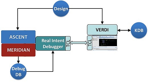 In this flow Verdi is invoked from the Real Intent Debugger. If Verdi is
being launched for the first time on a design, a number of actions take
place automatically in the background for proper setup: a one-time compile
of the design into Verdi's KDB database is done using vericom or vhdlcom
(depending on the kind of HDL code); and a one-time write of the novas.rc
file to silence warnings; and it loads Real Intent's custom function libs.
The TCL interpreter in the Real Intent debugger supports a bi-directional
socket with the TCL interpreter in Verdi. As a design engineer traces
through his design in Verdi, the appropriate debug information is pulled
through the TCL socket and displayed in the GUI.
For debugging, the Real Intent interface has Verdi draw pruned schematics
so the users see the violation context only. Visual enhancements are used
to aid debug:
- Color signals to identify clock domains.
- Stars and text tags to annotate violation targets.
- Colors and text tags to highlight special signals
like resets, clocks, and constants.
To support high-performance drawing of pruned schematics, Real Intent has
two custom TCL libraries. The first library on the Real Intent debugger
side implements advanced tracing functionality. The second lib is on the
Verdi side -- it's a TCL source lib to extend functionality and speeds up
computations.
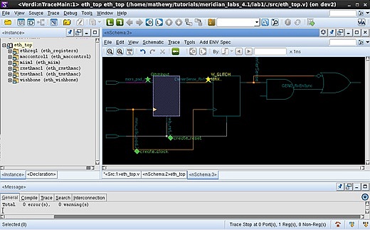
Mathew illustrated the operation of the tool using the Real Intent debugger
on a report from the Meridian CDC clock domain crossing tool. By double-
clicking on the warning in the Real Intent Debugger, Verdi is automatically
launched with the debug information shown below:
In this flow Verdi is invoked from the Real Intent Debugger. If Verdi is
being launched for the first time on a design, a number of actions take
place automatically in the background for proper setup: a one-time compile
of the design into Verdi's KDB database is done using vericom or vhdlcom
(depending on the kind of HDL code); and a one-time write of the novas.rc
file to silence warnings; and it loads Real Intent's custom function libs.
The TCL interpreter in the Real Intent debugger supports a bi-directional
socket with the TCL interpreter in Verdi. As a design engineer traces
through his design in Verdi, the appropriate debug information is pulled
through the TCL socket and displayed in the GUI.
For debugging, the Real Intent interface has Verdi draw pruned schematics
so the users see the violation context only. Visual enhancements are used
to aid debug:
- Color signals to identify clock domains.
- Stars and text tags to annotate violation targets.
- Colors and text tags to highlight special signals
like resets, clocks, and constants.
To support high-performance drawing of pruned schematics, Real Intent has
two custom TCL libraries. The first library on the Real Intent debugger
side implements advanced tracing functionality. The second lib is on the
Verdi side -- it's a TCL source lib to extend functionality and speeds up
computations.
Mathew illustrated the operation of the tool using the Real Intent debugger
on a report from the Meridian CDC clock domain crossing tool. By double-
clicking on the warning in the Real Intent Debugger, Verdi is automatically
launched with the debug information shown below:
 Future developments include extending the use of annotations and highlights
for Real Intent's Ascent XV X-verification tool.
- Graham Bell
Real Intent, Inc. Sunnyvale, CA
-----
John Cooley runs DeepChip.com, is a contract ASIC designer, and loves
hearing from engineers at or (508) 429-4357.
Future developments include extending the use of annotations and highlights
for Real Intent's Ascent XV X-verification tool.
- Graham Bell
Real Intent, Inc. Sunnyvale, CA
-----
John Cooley runs DeepChip.com, is a contract ASIC designer, and loves
hearing from engineers at or (508) 429-4357.
|
|