( ESNUG 561 Item 3 ) -------------------------------------------- [05/27/16]

Subject: Cooley trying to grok those funky litho/TCAD/process EDA tools
This 1926 Naval Academy cadet wrote some of the most influential
scifi in the 1940's through to 1970's.
Grok /'grok/ is a word coined by Robert A. Heinlein for his 1961 science-fiction
novel "Stranger in a Strange Land". While the Oxford English Dictionary
summarizes the meaning of grok as "to understand intuitively or by empathy, to
establish rapport with" and "to empathize or communicate sympathetically (with);
also, to experience enjoyment", Heinlein's concept is far more nuanced...
- from https://en.wikipedia.org/wiki/Grok
From: [ John Cooley of DeepChip.com ]

It was a lazy rainy Sunday afternoon in Boston, so my girlfriend wanted to
stay inside cooking and watching that dreadfully boring Food Network.
"This is great!  We can have some *together* time today!!!", she says.
And there's only so many times I can watch a chubby white guy with a bad
blonde dye job gush about how neat it was to fry a hamburger on TV before
I zoned out.  So I quietly borrowed my girlfriend's iPad.  Somehow, after
some random unrelated browsing, I found myself reading the SUNY Polytech
conference program to the 2015 Albany Nanotech Symposium.
Some IBM bigwig gave a keynote chatting up the "Apple-IBM Ecosystem" (huh?)
followed by a parade of IBM and GlobalFoundries process guys talking about
14nm and 10nm process stuff.  Oh, wow!  Each talk was only 5 minutes long!

"You're still sooooo over your head now, Cooley!", I thought to myself.
But then I found a Coventor paper. I know that name Coventor! They were at
DAC last year. And anyway, how lost can I get in a 5 minute paper?
"Extreme Ultraviolet Mask Blank Defect Evolution Study with SEMulator3D"
Blah blah EUV lithography. Blah blah defect-free EUV mask blanks are far
from reality blah blah. Simulate the growth of multilayer over a defect.
[OK, so the EDA part is simulating how wafers are made I guess.] Blah blah
transmission electron microscopy (TEM) & atomic force microscopy (AFM) blah
blah. Model using the Coventor SEMulator3D tool... TEM images for both
bump and pit type defects... Blah blah multilayer growth of 40 layers each
of alternating Mo and Si layers blah blah blah...
OK, so they're modeling how bumps and pits look after 80 layers of stuff is
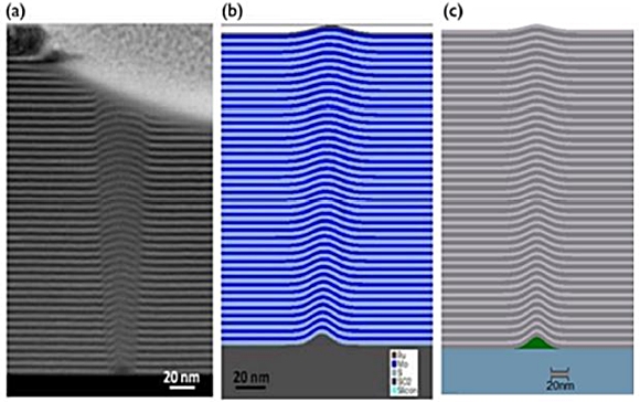
grown on top of them. Here's what the bump defect looks like:
Left is the real life wafer stack. Middle is what "level-set" multilayer
predicts. Right is what Coventor SEMulator3 predicted for the bump.
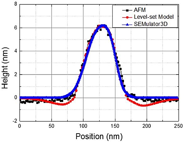
Here's the graph showing the same bump data:
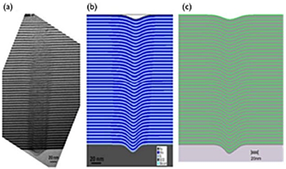
Now here's what the pit defect looks like:
Left is the real life wafer stack. Middle is what "level-set" multilayer
predicts. Right is what Coventor SEMulator3 predicted for the pit.
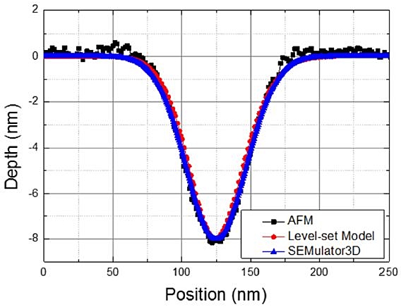
Here's the graph showing the same pit data:
So, the 5 minute story in a nutshell, the Coventor EDA process tool worked.
That is, it actually modeled in 3-D how Si wafers are actually fabbed.

        ----    ----    ----    ----    ----    ----    ----

Hmmm....

Then a whole bunch of Coventor questions started popping up in my head:

  - Why do you need SW to predict how bumps and pits look on a wafer?
    Isn't this already known from trillions of wafer fabbed before?
    Why are Intel/GF/TSMC/insert-other-big-fab-names-here using it?

  - With all this litho/wafer simulation stuff, why is "MEMS" liberally
    spread all across the Coventor web site?  Are they only for "MEMS"
    silicon stacks?  Analog/digital/AMS need not apply?

  - At what point does this Coventor process fab simulation tool crap
    out because of upcoming crazy physical effects?  7nm?  5nm?  3nm?
    Won't weird quantum physics eventually kick in ruining this?

Then I drifted off into other litho/TCAD/process EDA tool questions:

  - Wally has Calibre; which is waaaay deep into the BEOL/FOEL world.
    Googled "Calibre litho", some tool called "Calibre LFD" comes up.
    And Calibre nmOPC.  And RET.  What are all those about?

  - Didn't Mentor buy Pyxis to do "MEMS" PnR?  Did Pyxis die off?

  - Googled "Cadence litho".  Cadence Litho Physical Analyzer, Litho
    Electrical Analyzer, and DFM Services came up?  I didn't even
    know that Cadence did anything in the litho space!!!

  - Googled "Synopsys litho".  I found that Aart has Proteus WorkBench
    and Sentaurus.  What are those all about?

  - Oh, and then I remembered ClearShape that Cadence bought in 2007.
    DFM was hot in 2006.  It even had its own special ESNUG Post 453,
    followed by a lot of ClearShape chatter ESNUG 467 #6, ELSE'06 #22,
    Wiretap 070627, ESNUG 463 #6.  Did ClearShape die out after it got
    acquired by Cadence?

  - What's the differences between Silvaco TCAD and Synopsys TCAD?
    Is it just pricing?  Or a just node difference, with Silvaco
    being 32nm TCAD on up?  And Synopsys being 28nm TCAD on down?

  - Aart just bought Gold Standard Simulations, Ltd. which does TCAD
    variation models -- how does this impact Silvaco TCAD?

  - Also, why aren't MENT and CDNS in TCAD?

  - And what are these Sage iDRM, and Xalis, and EdXact Jivaro physical
    deep backend and/or fab tools showing at DAC all about?

Oh, man.  It was just too much of a distraction before I had to get back to
work on my upcoming DAC Cheesy Must See List for Austin. ...
Oh, look.  That chubby-bad-hair-dye guy is grilling more meat on the TV...

    - [ John Cooley of DeepChip.com ]
Join
Index
Next->Item
|
|