( ESNUG 518 Item 1 ) -------------------------------------------- [02/01/13]
Subject: CDNS admits rumor was right about Virtuoso ADE 12.X tool spilt
> - In reaction to Synopsys acquiring SpringSoft (and its Laker full
> custom layout tool), it's rumored that Cadence has split its
> Virtuoso into two new segments: IC6.X and IC12.X -- the thinking
> being that Virtuoso ADE 12.X will have twice the features that
> 6.X has. (Get it? 12.X is twice 6.X) The "new", pricier IC12.X
> will have all sorts of sexy 20 nm features like colorization,
> FinFET thingys, and double patterning; whereas the cheaper IC6.X
> will remain the cheaper basic model.
>
> (What doesn't make sense about this is ADE is already in three
> flavors: -G, -XL, and- GXL. Does this mean there will now to be
> six flavors of Virtuoso???)
>
> The rationale is to give Cadence Sales more flexibility in levels
> of ADE it offers designers to keep Synopsys full custom at bay.
>
> - from http://www.deepchip.com/items/0513-03.html
From: [ John Stabenow of Cadence ]
Three months ago, you leaked in your "News & Rumors" a hint about Virtuoso
and the new versions of it coming out. Now that the press release is out,
let me give you a little clarification.
You said that we have a "12.1" release. This is the Virtuoso Advanced Node
release that was in the press release this week. Why the name "12.1"? It's
really more simple than anyone would think -- it was first shipped in 2012,
and was release #1 (12.1).
While I liked that you said it "twice the features", the reason for the
Virtuoso Advanced Node release is more about use model than anything else.
From selling full custom layout SW to designers for the past 30 years, we've
known the standard flow has been to:
1.) The circuit designer designs a circuit design in Composer,
2.) maybe does some intelligent estimation of parasitics pre-layout,
then hands it off to the layout designer.
3.) Layout designer then does the layout, and once it is LVS/DRC clean,
does an extraction and
4.) passes it back to the circuit designer to resimulate in SPICE.
Typical iterations are 0 for exceptional design teams (or those who have
developed work-arounds for layout parasitics), up to 10 times for designs
that are very sensitive to small layout effects.
Once you hit 20 nm, this full custom design hand-off flow breaks down
horribly. Instead it must be done collaboratively since every choice made
in terms of the physical implementation has a significant effect on the
overall success of the design. Virtuoso Advanced Node and its special use
of Double Patterning (DPT) is critical to creating manufacturable parts.
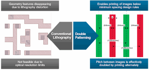 Double Patterning works by alternate printing
To add yet another wrinkle, using Double Patterning is causing layout times
to explode for many of our customers. How they react to this increased
layout time falls into two camps:
1.) The "we do not care about DPT" camp. They use design rules
that are the same mask rules (more loose) or they transition
to non-DPT metal layers as fast as they can. They pay a penalty
in area, but they avoid the elongated layout design times.
2.) The other camp is pushing 20 nm to be as tight as possible.
There, I have heard layout can take anything from 2x to 10x
longer to do. Imagine a 4 hour flop (std cell) layout taking
40 hours!
To help the second camp, we developed the ability to do color as you draw
(i.e. ensure a layout is decomposable). Double patterning splits the design
layers into two masks, separating structures that are too close together.
However, this double patterning brings "coloring" headaches to designers.
To fix this, Virtuoso Advanced Node does real-time automated color-aware,
design-rule-driven layout that let's you do area-optimized layout. You
1.) match, lock and store colors on critical nets and geometries
(through schematic constraints or directly on the layout), and
2.) identify, debug and fix errors as they go -- rather than later
in the design process, when they are more difficult to fix.
Again, this is done in TWO parts -- using our new Design Rule Driven (DRD)
engine in Virtuoso to prevent as many errors as possible, and the PVS
real-time integration to Virtuoso (IPVS) to detect any DRC errors upon the
finish of any given edit. (DRD is good, and can cover a lot of issues, but
you need a sign-off quality check at the end of each edit - thus the need
for IPVS.)
LOCAL INTERCONNECT
There is another "new" issue, Local Interconnect (LI). OK, for the record,
LI is not new. I have seen it in use at 180 nm. But, for 20 nm and below,
it's no longer an option. LI is a layer between metal1 and the transistors.
Foundries require the new local interconnect (LI) layers, or middle-of-line
(MOL) layers, to create densely packed routes inside complex devices.
Double Patterning works by alternate printing
To add yet another wrinkle, using Double Patterning is causing layout times
to explode for many of our customers. How they react to this increased
layout time falls into two camps:
1.) The "we do not care about DPT" camp. They use design rules
that are the same mask rules (more loose) or they transition
to non-DPT metal layers as fast as they can. They pay a penalty
in area, but they avoid the elongated layout design times.
2.) The other camp is pushing 20 nm to be as tight as possible.
There, I have heard layout can take anything from 2x to 10x
longer to do. Imagine a 4 hour flop (std cell) layout taking
40 hours!
To help the second camp, we developed the ability to do color as you draw
(i.e. ensure a layout is decomposable). Double patterning splits the design
layers into two masks, separating structures that are too close together.
However, this double patterning brings "coloring" headaches to designers.
To fix this, Virtuoso Advanced Node does real-time automated color-aware,
design-rule-driven layout that let's you do area-optimized layout. You
1.) match, lock and store colors on critical nets and geometries
(through schematic constraints or directly on the layout), and
2.) identify, debug and fix errors as they go -- rather than later
in the design process, when they are more difficult to fix.
Again, this is done in TWO parts -- using our new Design Rule Driven (DRD)
engine in Virtuoso to prevent as many errors as possible, and the PVS
real-time integration to Virtuoso (IPVS) to detect any DRC errors upon the
finish of any given edit. (DRD is good, and can cover a lot of issues, but
you need a sign-off quality check at the end of each edit - thus the need
for IPVS.)
LOCAL INTERCONNECT
There is another "new" issue, Local Interconnect (LI). OK, for the record,
LI is not new. I have seen it in use at 180 nm. But, for 20 nm and below,
it's no longer an option. LI is a layer between metal1 and the transistors.
Foundries require the new local interconnect (LI) layers, or middle-of-line
(MOL) layers, to create densely packed routes inside complex devices.
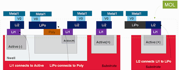 Li1, Li2, LiPo are all LI between metal1 and transistors
LI layers have restricted design rules governing local interconnect and
the vias that are used with them, creating the headache of maintaining
signal integrity from pin-to-pin in transistors. Virtuoso Advanced Node
has a local interconnect-aware wire editor and a LI-rules-friendly router.
IC6.X vs. IC12.X
So back to "why Virtuoso Advanced Node" -- there are so many designer tool
use model changes needed to accommodate DPT layout problems -- like DRD,
but also the wire editor (use of local interconnect), the auto device
placers and abutment engines (dummy poly rules), and how color data is
stored in OA. To make sure that the vast majority of the Virtuoso user
base who is NOT on 20 nm does not see their tool use model change, we have
separated Virtouso for two types of users (DPT and not-DPT).
IC 6.1.5 is still our mainstream release, and we are enhancing it for all
of our design community. IC 12.X (Virtuoso Advanced Node) is the release
for 20 nm and below -- and its users will see more and more go into it as
new challenges like FinFET's come on line. Both IC6.X and IC12.X will
remain SKILL compatible and OA database compatible.
STARTED 18 MONTHS AGO
One other small point. The work we've been doing on Virtuoso Advanced Node
started more than 18 months ago. The answer to your question of "was this
in response to a competitors move". No. This entire effort was driven by
close collaborations with TSMC/Samsung/IBM/GlobalFoundries and with our
Customers who are on the leading edge of process technologies. We've been
trading ideas, working through test chips and co-presenting on IC12.X at
industry events for quite some time.
- John Stabenow
Cadence Design Systems, Inc. San Jose, CA
Editor's Note: If you look halfway down ESNUG 510 #1, John Murphy
also detailed how Double Patterning (DPT) works in IC12.X. - John
Li1, Li2, LiPo are all LI between metal1 and transistors
LI layers have restricted design rules governing local interconnect and
the vias that are used with them, creating the headache of maintaining
signal integrity from pin-to-pin in transistors. Virtuoso Advanced Node
has a local interconnect-aware wire editor and a LI-rules-friendly router.
IC6.X vs. IC12.X
So back to "why Virtuoso Advanced Node" -- there are so many designer tool
use model changes needed to accommodate DPT layout problems -- like DRD,
but also the wire editor (use of local interconnect), the auto device
placers and abutment engines (dummy poly rules), and how color data is
stored in OA. To make sure that the vast majority of the Virtuoso user
base who is NOT on 20 nm does not see their tool use model change, we have
separated Virtouso for two types of users (DPT and not-DPT).
IC 6.1.5 is still our mainstream release, and we are enhancing it for all
of our design community. IC 12.X (Virtuoso Advanced Node) is the release
for 20 nm and below -- and its users will see more and more go into it as
new challenges like FinFET's come on line. Both IC6.X and IC12.X will
remain SKILL compatible and OA database compatible.
STARTED 18 MONTHS AGO
One other small point. The work we've been doing on Virtuoso Advanced Node
started more than 18 months ago. The answer to your question of "was this
in response to a competitors move". No. This entire effort was driven by
close collaborations with TSMC/Samsung/IBM/GlobalFoundries and with our
Customers who are on the leading edge of process technologies. We've been
trading ideas, working through test chips and co-presenting on IC12.X at
industry events for quite some time.
- John Stabenow
Cadence Design Systems, Inc. San Jose, CA
Editor's Note: If you look halfway down ESNUG 510 #1, John Murphy
also detailed how Double Patterning (DPT) works in IC12.X. - John
Join
Index
Next->Item
|
|